Optical integrated device and optical control device

a technology of optical control device and integrated device, which is applied in the direction of optical waveguide light guide, optical elements, instruments, etc., can solve the problems of large device size of silicon-based waveguide, inability to meet high integration, and inability to absorb light scattering, etc., and achieve easy fabricability of optical coupling parts and low loss

Inactive Publication Date: 2007-02-15
RICOH KK
View PDF6 Cites 31 Cited by
  • Summary
  • Abstract
  • Description
  • Claims
  • Application Information

AI Technical Summary

Benefits of technology

[0014] Embodiments of the present invention may solve or reduce one or more of the above problems.
[0016] According to one embodiment of the present invention, a high-density, low-loss optical integrated device and optical control device are provided by providing a low index difference waveguide and a high index difference waveguide on the same substrate and connecting the waveguides at an optical coupling part.
[0018] Accordingly, it is possible to provide an easily fabricable, low-loss optical integrated device in which optical waveguides disposed on the same substrate are integrated with high density.
[0020] Accordingly, it is possible to provide an easily fabricable, low-loss optical integrated device in which optical waveguides disposed on the same substrate are integrated with high density.
[0022] Accordingly, it is possible to provide an optical integrated device that couples optical waveguides having different relative index differences with low loss and includes an easily fabricable optical coupling part.

Problems solved by technology

As a result, the silica-based waveguide is large in device size, and therefore, is not suitable for high integration.
However, although a total reflection linear waveguide can perform lossless light propagation in principle, propagation loss is inevitably caused by light scattering due to the roughness of the side faces of the waveguide (core) generated at the time of its fabrication.
Accordingly, there is a problem in that in the case of configuring an optical integrated circuit formed of multiple optical control devices of an optical waveguide type using only HIC optical waveguides, or in the case of including a linear portion in the device structure, the insertion loss of the entire integrated circuit is extremely great.
However, in realizing such a layered optical waveguide device, there is a problem in that the fabrication process is complicated and that it is very difficult align an optical interconnection and an optical control part.

Method used


Image

  • Optical integrated device and optical control device
  • Optical integrated device and optical control device
  • Optical integrated device and optical control device

Examples


first embodiment

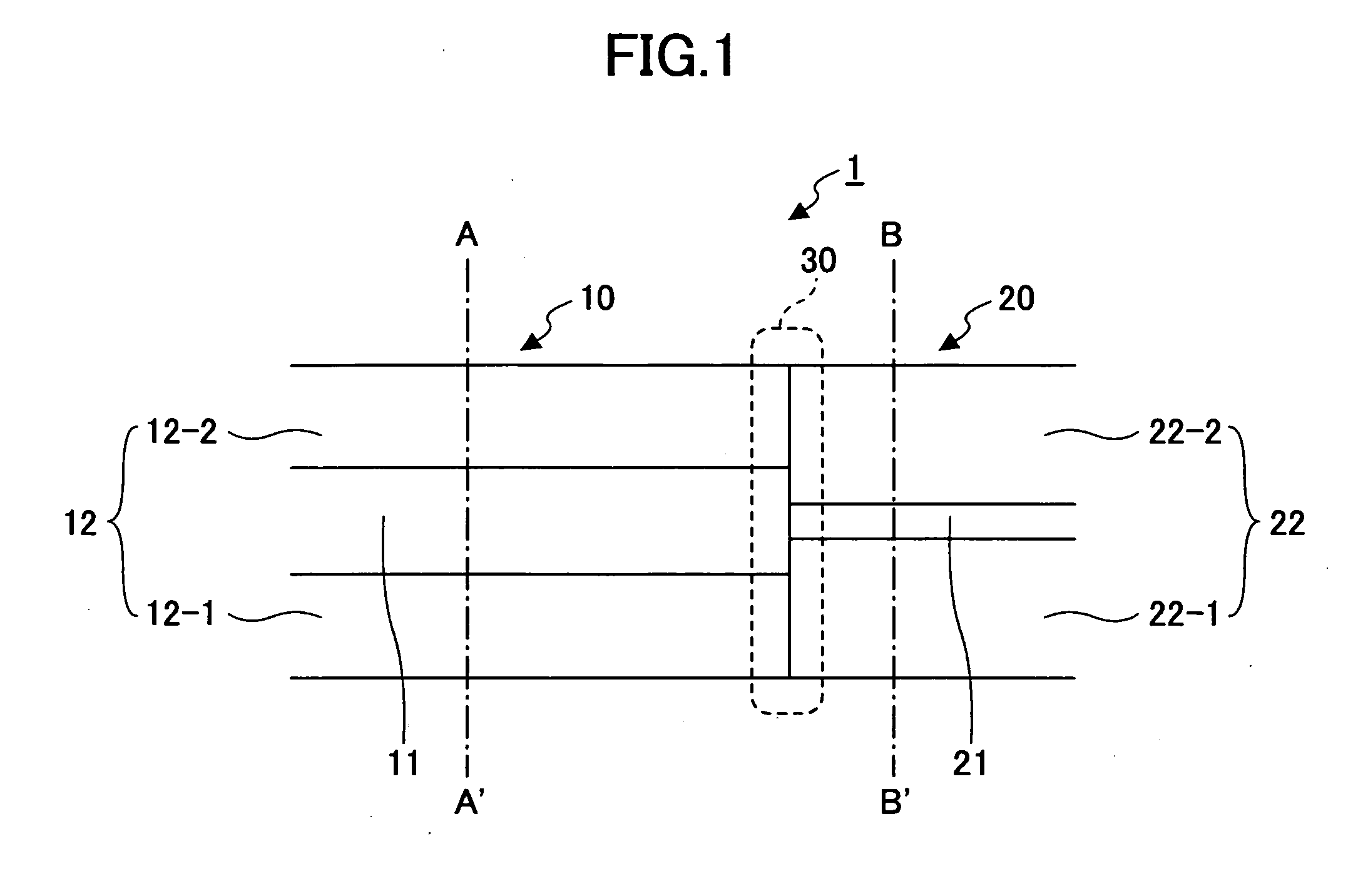
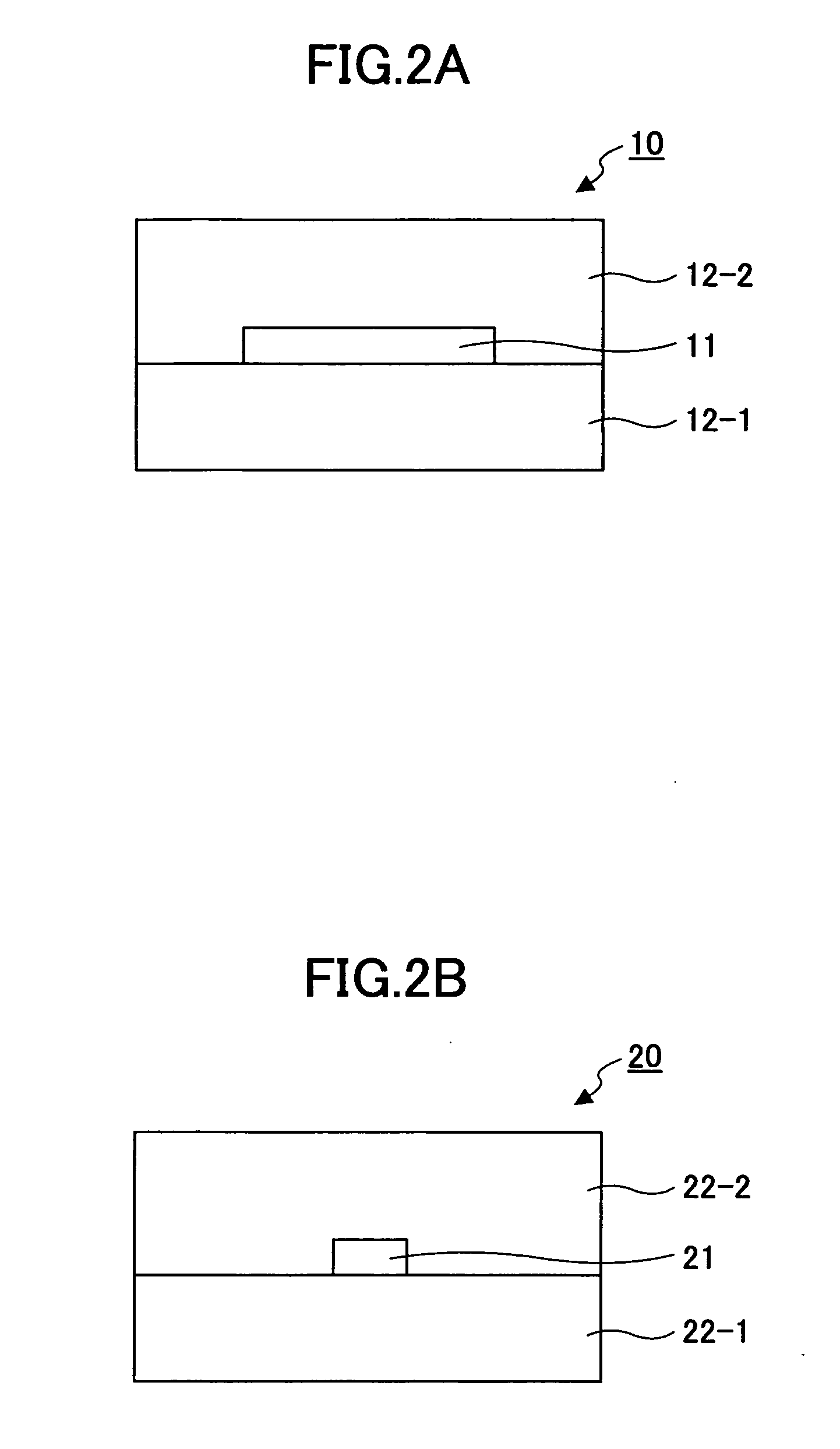
[0062]FIG. 1 is a sectional view of an optical integrated device 1 according to the present invention. Referring to FIG. 1, the optical integrated device 1 includes an optical waveguide 10 and an optical waveguide 20 that propagate light. The optical waveguides 10 and 20 are formed and coupled to each other on the same substrate. The optical waveguide 10 includes a core 11 and a cladding 12. The core 11 is higher in refractive index than the cladding 12, thereby confining light in the core 11 using total reflection and propagating light. Further, the optical waveguide 20 includes a core 21 and a cladding 22. Light propagates in the core 21 in the optical waveguide 20 the same as in the optical waveguide 10. The optical integrated device 1 has an optical coupling part 30 at which the optical waveguide 10 and the optical waveguide 20 are coupled in series. The light that propagates in the optical waveguide 10 is coupled to the optical waveguide 20 through the optical coupling part 30 ...

second embodiment

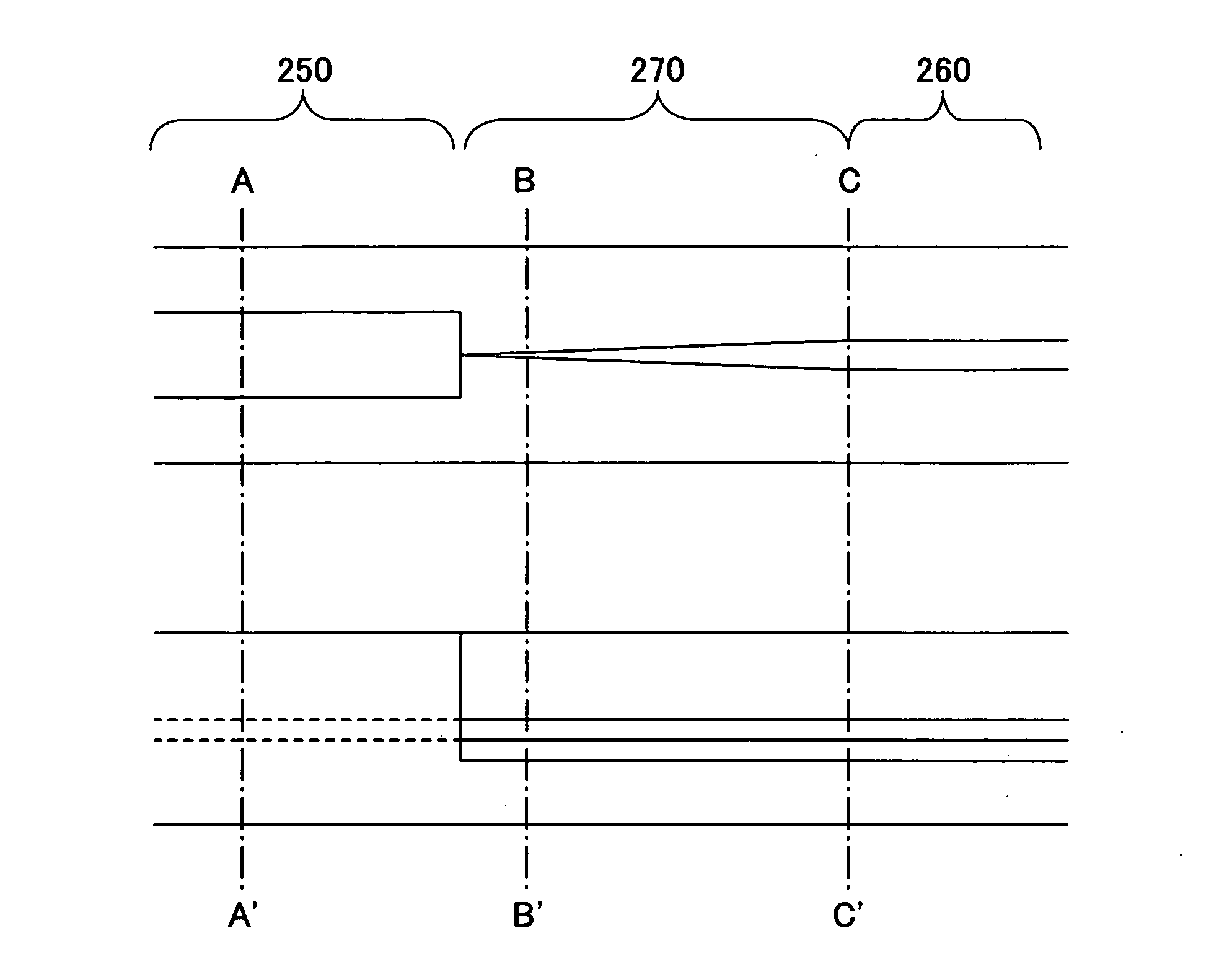
[0067]FIG. 3 is a sectional view of an optical integrated device 2 according to the present invention. The optical integrated device 2 of this embodiment shown in FIG. 3 has a configuration where three types of waveguides are integrated. Referring to FIG. 3, optical waveguides 40, 50, and 60 are connected in order in series. The optical waveguides 40 and 50 are coupled by an optical coupling part 70, and the optical waveguides 50 and 60 are coupled by an optical coupling part 80. Here, the optical waveguide 40 and the optical waveguide 60 have the same relative index difference, which is different from the relative index difference of the optical waveguide 50. According to this embodiment, the optical waveguide 50 is a high index difference waveguide, and the optical waveguides 40 and 60 are low index difference waveguides. Alternatively, however, the optical waveguide 50 may be a low index difference waveguide, and the optical waveguides 40 and 60 may be high index difference waveg...

third embodiment

[0069]FIG. 4 is a sectional view of an optical integrated device 3 according to the present invention. In FIG. 4, the same elements as those of FIG. 3 are referred to by the same reference numerals. The optical integrated device 3 integrates three types of waveguides. In the optical integrated device 3, the optical waveguide 50 is a high index difference waveguide, and the optical waveguides 40 and 60 are low index difference waveguides. Further, the optical waveguide 50 includes a curved part 51 as shown in FIG. 4. Since the optical waveguide 50 is strong in light confinement, it is possible to reduce a radius of curvature at the curved part 51. As a result, the direction of light propagation in the low index difference waveguide can be changed in an extremely minute region. In the case of FIG. 4, the optical waveguide 40 and the optical waveguide 60, which are low index difference waveguides, are linear waveguides. Alternatively, the same effect can be produced by providing the op...


PUM


Abstract

An optical integrated device having multiple optical waveguides connected on the same substrate and each including a core and a cladding is disclosed. Adjacent two of the optical waveguides are different in the refractive index difference between the core and the cladding.

Description

BACKGROUND OF THE INVENTION [0001] 1. Field of the Invention [0002] The present invention relates generally to optical integrated devices and optical control devices, and more particularly to an optical integrated device having optical waveguides different in refractive index difference coupled to each other, and to an optical control device using the same. Examples of the optical control device include an optical delay device, an optical switching device, an optical routing device, an optical information processor, a light emitting device, a light receiving device, and a non-linear optical device. [0003] 2. Description of the Related Art [0004] Optical integrated circuits employing a planar lightwave circuit (PLC) as a basic interconnection element are capable of advanced optical signal control, and are principal components in optical communications. Many of the optical circuits employed in these optical integrated circuits have a waveguide structure confining light in a core using...

Claims


Application Information

Patent Timeline
Patent Type & Authority Applications(United States)
IPC IPC(8): G02B6/10
CPCB82Y20/00G02B6/12004G02B6/1223G02B2006/12164G02B6/305G02B2006/12119G02B2006/12147G02B6/1228
Inventor SUZUKI, SHUICHISAKAI, ATSUSHI
Owner RICOH KK
Why Eureka
Try Eureka