Silicon based condenser microphone and packaging method for the same
a condenser microphone and silicon-based technology, applied in the field of condenser microphones, can solve the problems of deterioration of bonding properties and increase of manufacturing costs, and achieve the effect of increasing bonding strength and high resistance to external nois
- Summary
- Abstract
- Description
- Claims
- Application Information
AI Technical Summary
Benefits of technology
Problems solved by technology
Method used
Image
Examples
embodiment 1
Modification 1 of Embodiment 1
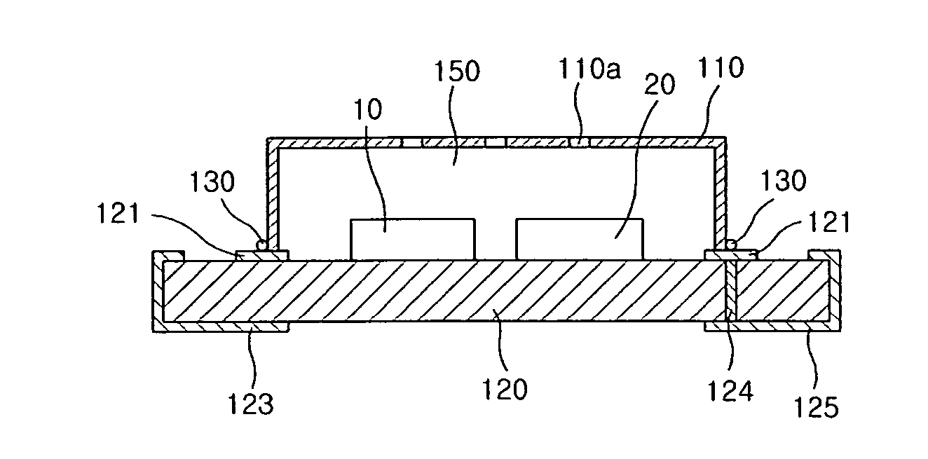
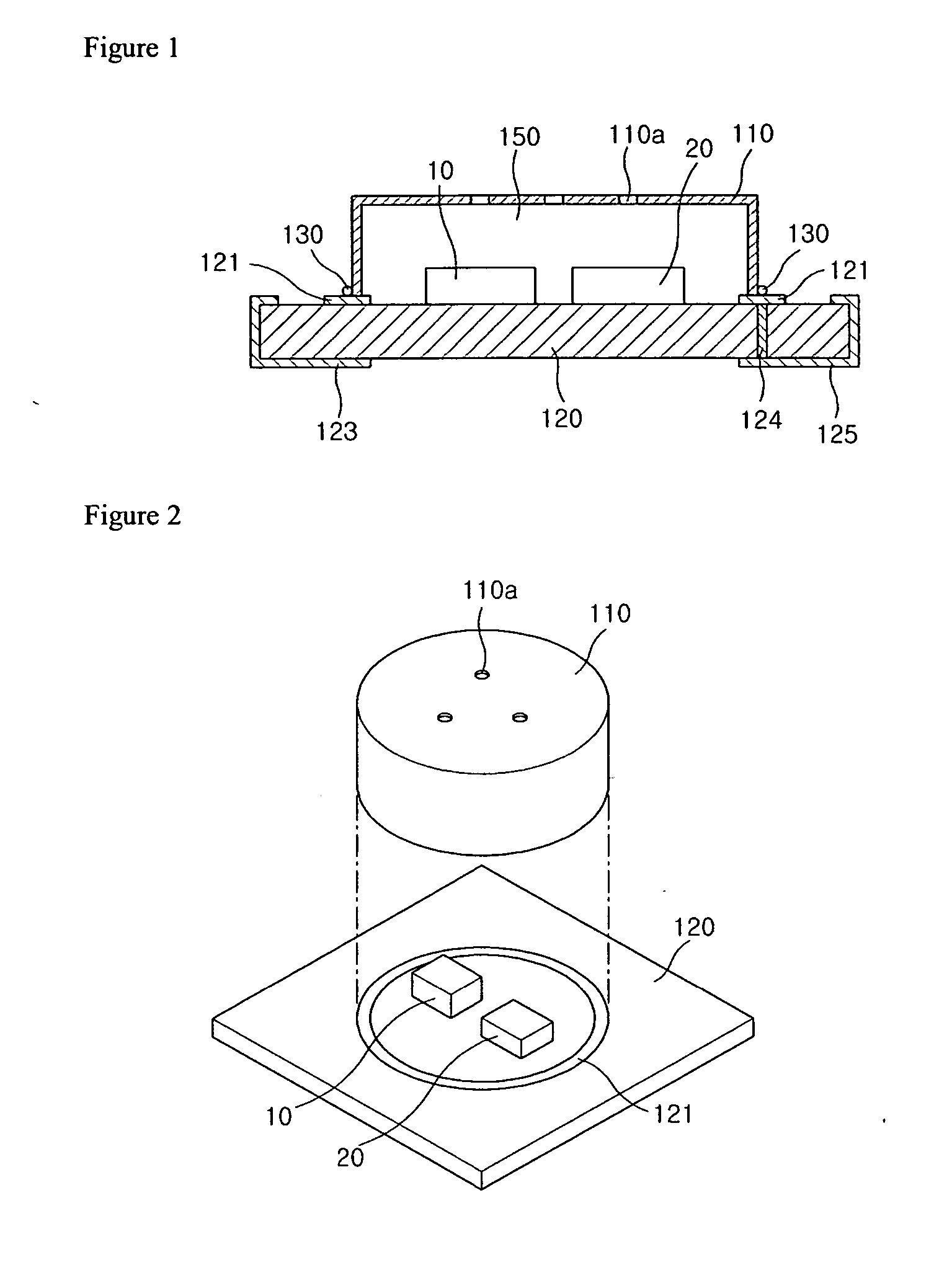
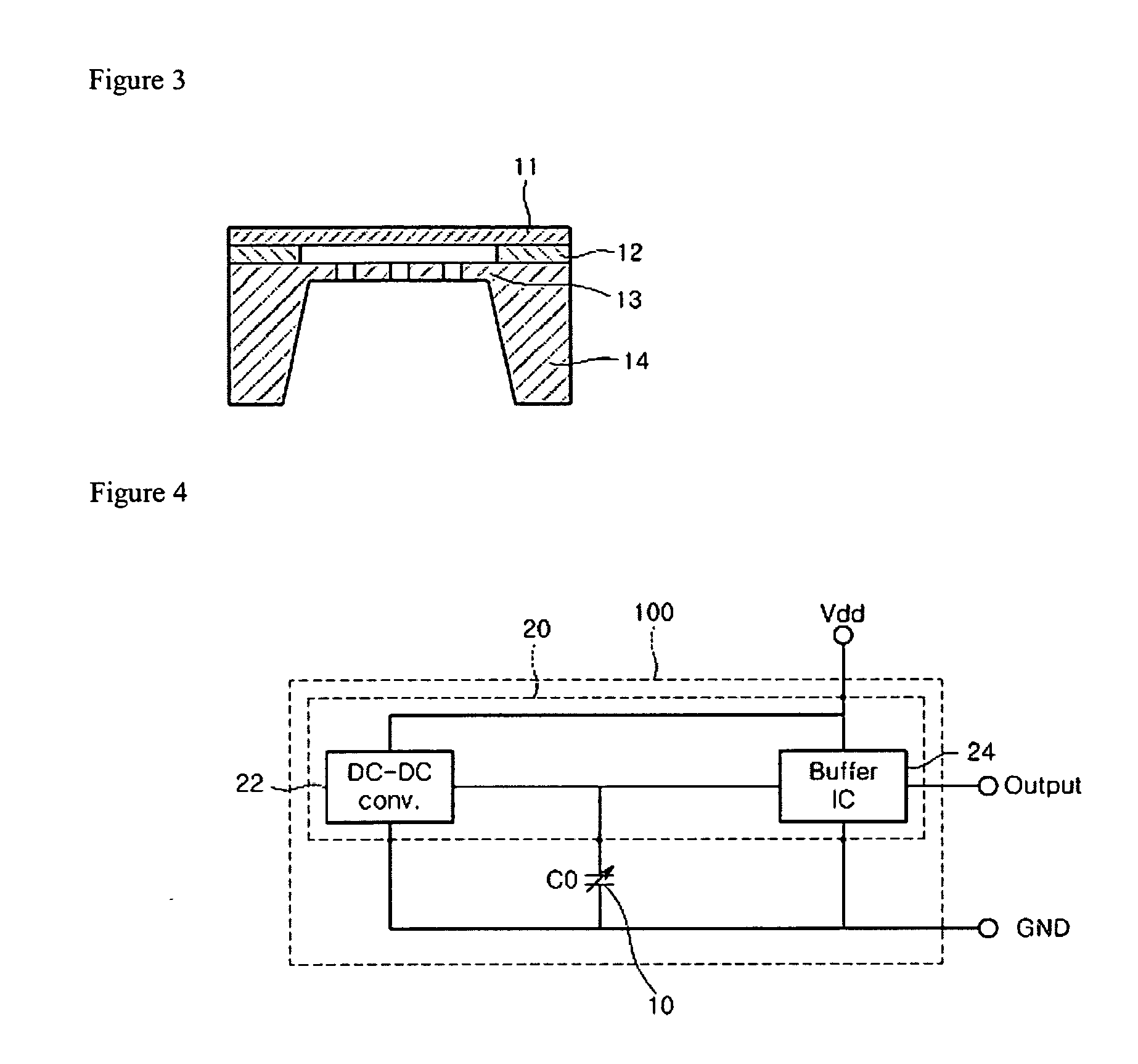
[0038]FIG. 1 is a sectional side view of a first modification of a first embodiment according to the present invention, FIG. 2 is an exploded perspective view of a first modification of a first embodiment according to the present invention, FIG. 3 is a view showing an example of a structure for a MEMS chip of a silicon based condenser microphone applied to each embodiment of the present invention in common, and FIG. 4 is a circuit diagram of a silicon based condenser microphone according to the present invention.
[0039] According to a first modification of a first embodiment, as shown in FIGS. 1 and 2, a cylindrical metal case 110 is welded to a PCB 120 which is mounted with a MEMS chip 10 and an ASIC chip 20 by a laser.
[0040] Referring to FIGS. 1 and 2, the PCB 120 is mounted with the MEMS chip 10 and the ASIC chip 20 and is formed with a circular connecting pattern 121 on a portion which contacts the metal case 110. Meanwhile, if necessary, the PCB ...
embodiment 2
Modification 1 of Embodiment 2
[0069]FIG. 10 is a sectional side view of a first modification of a second embodiment according to the present invention, FIG. 11 is a sectional side view showing that a microphone shown in FIG. 10 is mounted on a main PCB, and FIG. 12 is an exploded perspective view of a first modification of a second embodiment according to the present invention.
[0070] According to a first modification of a second embodiment according to the present invention, as shown in FIGS. 10 and 12, there is provided an example that a cylindrical metal case 110 is welded to a PCB 120 which is mounted with a MEMS chip 10 and an ASIC chip 20 by a laser.
[0071] Referring to FIGS. 10 and 12, the PCB 120 is formed with a sound hole 120a for collecting an external sound near the center thereof and is mounted with the MEMS chip 10 and the ASIC chip 20 around the center thereof. Further, the PCB is formed with a circular connecting pattern 121 on its portion which contacts the metal c...
modification 5
of Embodiment 2
[0090]FIG. 16 is a sectional side view of a fifth modification of a second embodiment according to the present invention, wherein a PCB is formed with a sound hole on a portion where a MEMS chip is positioned.
[0091] Referring to FIG. 16, the metal case 110 is firmly attached to the connecting pattern 121 of the PCB 120 which is mounted with the MEMS chip 10 and the ASIC chip 20 by laser welding.
[0092] Further, the PCB 120 is formed with the sound hole 120a for collecting an external sound on a position where the MEMS chip 10 is mounted, and is formed with the sealing terminal 120a for sealing the sound hole 120a by soldering on the outside of the sound hole to prevent distortion of a sound wave in a space between the main PCB 300 and the microphone. Further, the PCB 120 may be formed with the connecting terminals 123 and 125 for connecting with the external device on a bottom surface thereof, wherein the number of the connecting terminals 123 and 125 may be two to e...
PUM
 Abstract
Description
Claims
Application Information


