Semiconductor device

a technology of semiconductor devices and semiconductors, applied in the direction of semiconductor devices, basic electric elements, electrical appliances, etc., can solve the problems of reducing the quality of signals present in other parts, affecting the quality of signals, and not being able to secure sufficient impedance, so as to prevent degradation of signal quality, improve isolation in semiconductor devices, and improve isolation

Inactive Publication Date: 2007-03-01
PANASONIC CORP
View PDF9 Cites 5 Cited by
  • Summary
  • Abstract
  • Description
  • Claims
  • Application Information

AI Technical Summary

Benefits of technology

[0031] With this, as noise can be led to the outside part via the region with a low resistivity, it is possible to improve the isolation in the semiconductor device.
[0032] Thus, according to the semiconductor device in the present invention, it is possible to secure favorable isolation while preventing degradation of the quality of signals caused by noise and reducing a malfunction of a circuit. In addition, it is possible to reduce the malfunction of a circuit caused by latch-up while preventing increase in a chip area. In other words, the semiconductor device can be miniaturized while a stable circuit operation can be secured. Moreover, these effects are not limited by the frequency band, device for use, or the system of the semiconductor device.

Problems solved by technology

This signal becomes noise for circuits, chips, or devices other than the devices which generate the signal, and degrades quality of signals present in other parts.
In particular, the more the area reductions in module layout, and use of digital-analog mixed chips and single-chips in the RF or baseband have been promoted, the more remarkable this problem becomes.
Thus, for example, in the case where an RF signal with frequency equal to 800 MHz or more is used, it is not possible to secure sufficiently high impedance.
As a result, the signal easily propagates through the horizontal direction via a substrate region below trenches, and then the propagated signal again propagates through the upward direction, which causes an occurrence of a crosstalk.
Therefore, this semiconductor device can not secure favorable isolation.
Thus, in the case where an RF signal with frequency equal to 800 MHz or more is used, it is not possible to secure sufficiently high impedance.
As a result, a crosstalk occurs, and even with this semiconductor device, favorable isolation can not be realized.
However, the more the resistivity of the substrate increases, the more thermal noise generated in the substrate increases.
In addition, as crystal defect easily occurs when the substrate resistivity is high, latch-up caused by leakage current in a PN junction easily occurs, and the circuit operation becomes unstable.

Method used


Image

  • Semiconductor device
  • Semiconductor device
  • Semiconductor device

Examples


first embodiment

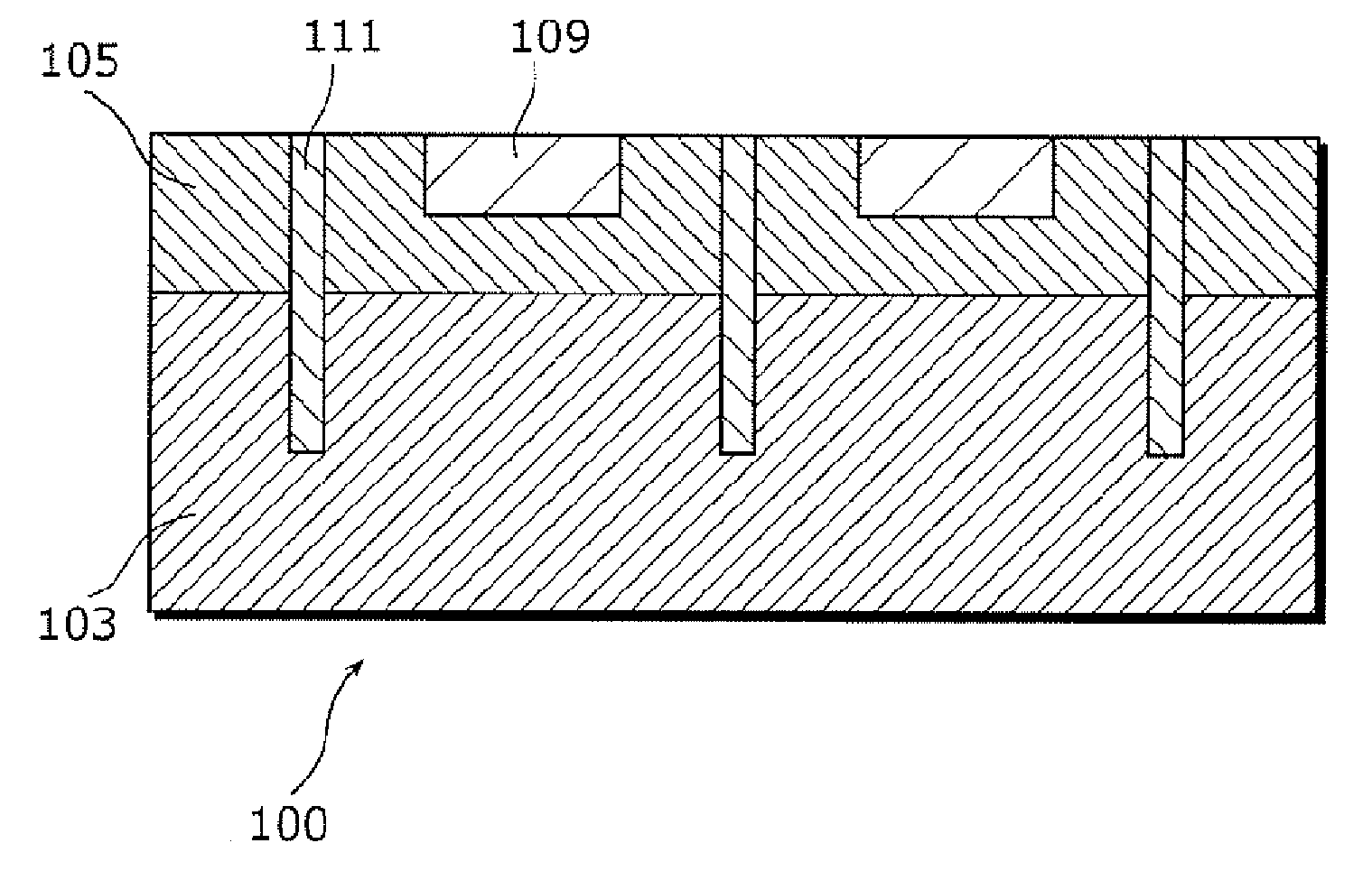
[0057]FIG. 4 is a cross sectional view showing a structure of the semiconductor device according to the first embodiment.

[0058] In this semiconductor device, a first layer 103, a second layer 105, and trench-type insulating regions 111 are formed in a semiconductor substrate 100.

[0059] The first layer 103 is a high resistivity substrate of a first conductivity type having a resistivity higher than 10 Ωcm and lower than 1 kΩcm, and is formed in the semiconductor substrate 100.

[0060] The second layer 105 is a low resistivity substrate of a second conductivity type having a resistivity lower than that of the first layer 103, for example, having low resistivity of 10 Ωcm, and is formed on a surface side in the semiconductor substrate 100 so as to be located above the first layer 103. In a predetermined part of the second layer 105, a plurality of semiconductor elements or semiconductor circuits (hereinafter simply referred to as semiconductor elements) 109 are formed. Moreover, the s...

second embodiment

[0077]FIG. 8 is a cross sectional view showing a structure of the semiconductor device according to the second embodiment.

[0078] This semiconductor device differs from the semiconductor device in the first embodiment in having first embedded layers 213 formed in the first layer 103 and second embedded layers 215 formed in the second layer 105.

[0079] The first embedded layer 213 is a second conductivity-type low resistivity layer having a resistivity lower than that of the first layer 103 so as to he formed in contact with the second layer 105.

[0080] The second embedded layer 215 is a second conductivity-type low resistivity layer having a resistivity lower than that of the first layer 103 and is formed so as to surround the semiconductor element 109 and be located between the trench-type insulating region 111 and the semiconductor element 109. The second embedded layers 215 vertically run from the surface of the semiconductor substrate 100 to the depth direction across the second...

third embodiment

[0084]FIG. 9 (a) is a top surface view of the semiconductor device according to the third embodiment, and FIG. 9 (b) is a cross sectional view of the same semiconductor device (cross sectional view in A-A′ line of FIG. 9 (a)).

[0085] This semiconductor device differs from the semiconductor device in the first embodiment in having a plurality of trench-type insulating regions between two semiconductor elements 109, in other words, having a first trench-type insulating region 311 and a second trench-type insulating region 321.

[0086] The first trench-type insulating region 311 and the second trench-type insulating region 321 are formed so as to surround each of the semiconductor elements 109, and electrically isolate the surrounded semiconductor element 109 from the other semiconductor elements 109. The first trench-type insulating region 311 and the second trench-type insulating region 321 vertically run from the surface of the semiconductor substrate 100 to the depth direction acros...


PUM


Abstract

The present invention aims at providing a semiconductor device that can prevent quality degradation of a signal caused by noise, reduce a malfunction of a circuit caused by latch-up, and secure favorable isolation, and the semiconductor device includes: a first layer with a resistivity higher than 10 Ωcm and lower than 1 kΩcm which is formed in a semiconductor substrate; a second layer formed on a surface of the semiconductor substrate so as to be located above the first layer; two semiconductor devices formed in the second layer or on the second layer; and a trench-type insulating region which is located between the two semiconductor devices, is formed in the semiconductor substrate so as to reach the first layer from the surface of the semiconductor substrate, and electrically isolates the two semiconductor devices.

Description

BACKGROUND OF THE INVENTION [0001] (1) Field of the Invention [0002] The present invention relates to a semiconductor device from a baseband to a radio frequency (RF) band, in which a semiconductor circuit and a semiconductor element provided in an analog circuit, a digital circuit or an analog-digital mixed circuit are formed, and particularly to a semiconductor device which prevents signal interference between elements or between blocks. [0003] (2) Description of the Related Art [0004] In recent years, there is a growing demand for miniaturizing and reducing the cost of modules used in a cellular phone, a mobile information terminal and the like. In response to such a demand, area reductions in chip layout, and use of single-chips in the RF or baseband and digital-analog mixed chips have been promoted. However, signal interference increases between elements, blocks, or chips in a semiconductor device with the aforementioned structure, and the interference hampers signal processing...

Claims


Application Information

Patent Timeline
Patent Type & Authority Applications(United States)
IPC IPC(8): H01L29/00
CPCH01L21/761H01L21/76224H01L29/7322H01L29/0821H01L27/0921
Inventor YAMANKA, MIKIHIRAOKA, YUKIOISHIKAWA, OSAMU
Owner PANASONIC CORP
Why Eureka
Try Eureka