Stacked chip package using warp preventing insulative material and manufacturing method thereof

a technology of insulating material and chip package, which is applied in the direction of semiconductor/solid-state device details, semiconductor devices, electrical equipment, etc., can solve the problems of high process throughput, large volume, and high cost of modern applications, and achieve the effect of preventing warping of semiconductor devices

Inactive Publication Date: 2007-03-01
SAMSUNG ELECTRONICS CO LTD
View PDF11 Cites 90 Cited by
  • Summary
  • Abstract
  • Description
  • Claims
  • Application Information

AI Technical Summary

Benefits of technology

[0010] The present invention provides for a stacked chip package configuration, and manufacturing methods thereof, wherein the gap between a lower chip and an upper chip is filled completely using a relatively simple process that eliminates voids, and the cracking and delamination problems associated with such voids. The present invention is applicable to both chip-level bonding and wafer-level bonding approaches. A photosensitive polymer layer is applied to a first chip, or wafer, prior to stacking the chips or stacking the wafers. The photosensitive polymer layer is partially cured, so that the photosensitive polymer layer is made to be structurally stable, while retaining its adhesive properties. The second chip, or wafer, is stacked, aligned, and bonded to the first chip, or wafer, and the photosensitive polymer layer is then cured to fully bond the first and second chips, or wafers. In this manner, adhesion between chips / wafers is greatly improved, while providing complete fill of the gap. In addition, mechanical reliability is improved and CTE mismatch is reduced, alleviating the problems associated with cracking and delamination. This leads to an improvement in device yield and device reliability.
[0045] In another embodiment, the first coefficient of thermal expansion of the photosensitive polymer layer being higher than the second coefficient of thermal expansion of the substrate compensates for active devices formed on a top portion of the substrate opposite the photosensitive polymer layer having a third coefficient of thermal expansion that is higher than the second coefficient of thermal expansion of the substrate, to prevent warping of the semiconductor device during subsequent thermal cycles of the semiconductor device.
[0063] In another embodiment, the first coefficient of thermal expansion of the first photosensitive polymer layer being higher than the second coefficient of thermal expansion of the first substrate compensates for active devices formed on a top portion of the first substrate opposite the first photosensitive polymer layer having a third coefficient of thermal expansion that is higher than the second coefficient of thermal expansion of the first substrate, to prevent warping of the semiconductor device during subsequent thermal cycles of the semiconductor device.

Problems solved by technology

The resulting MSPs enjoyed widespread use in the past, but are relatively bulky and cumbersome for modern applications.
The resulting MCPs have characteristically high yield, however, process throughput is a problem, as each individual chip needs to be handled during alignment and bonding processes.
The resulting WL CSPs suffer from low yield.
Chip level bonding and wafer level bonding are generally complicated and unstable manufacturing processes.
The underfill process is unreliable, since the gap between the lower and upper chip substrates is small, for example on the order of 20 μm.
If the underfill process does not result in a complete and uniform fill of the gap, then any resulting voids can increase the likelihood of future generation of cracks.
Such cracks can propagate during future heating and cooling cycles, decreasing the reliability of the resulting chip stack device.
Such stress is typically caused by a mismatch in coefficient of thermal expansion (CTE) between two adjacent layers.
Such CTE mismatch can cause further cracking and delamination when subjected to numerous heating and cooling thermal cycles, negatively affecting device yield during manufacture, and device reliability during operation.

Method used


Image

  • Stacked chip package using warp preventing insulative material and manufacturing method thereof
  • Stacked chip package using warp preventing insulative material and manufacturing method thereof
  • Stacked chip package using warp preventing insulative material and manufacturing method thereof

Examples


second embodiment

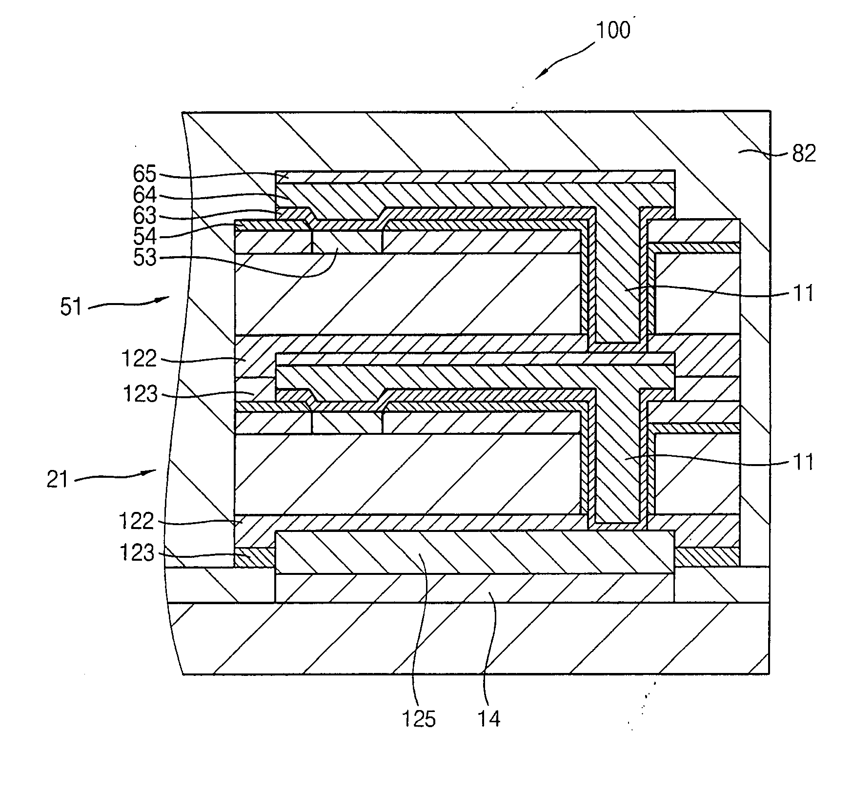
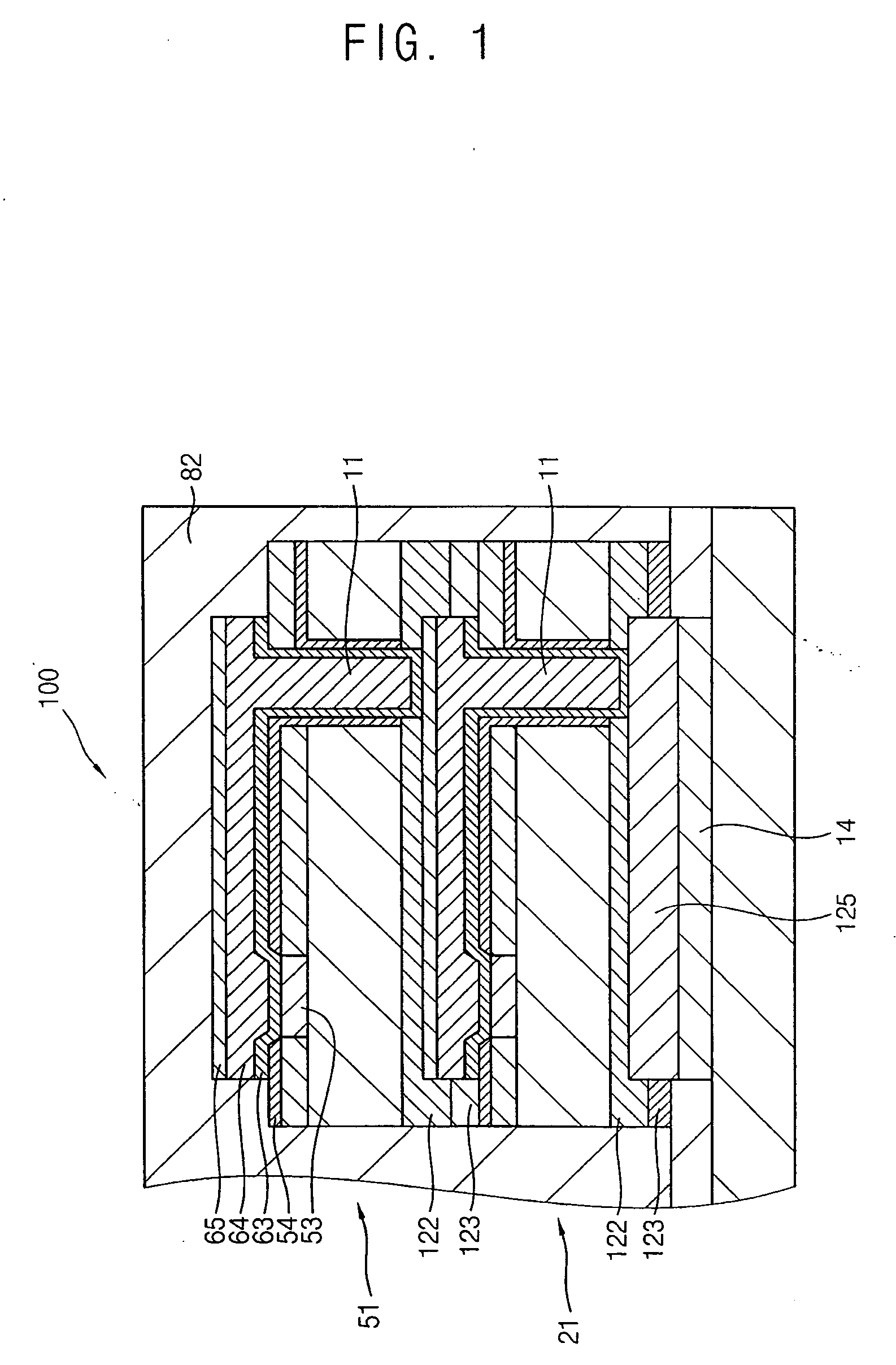
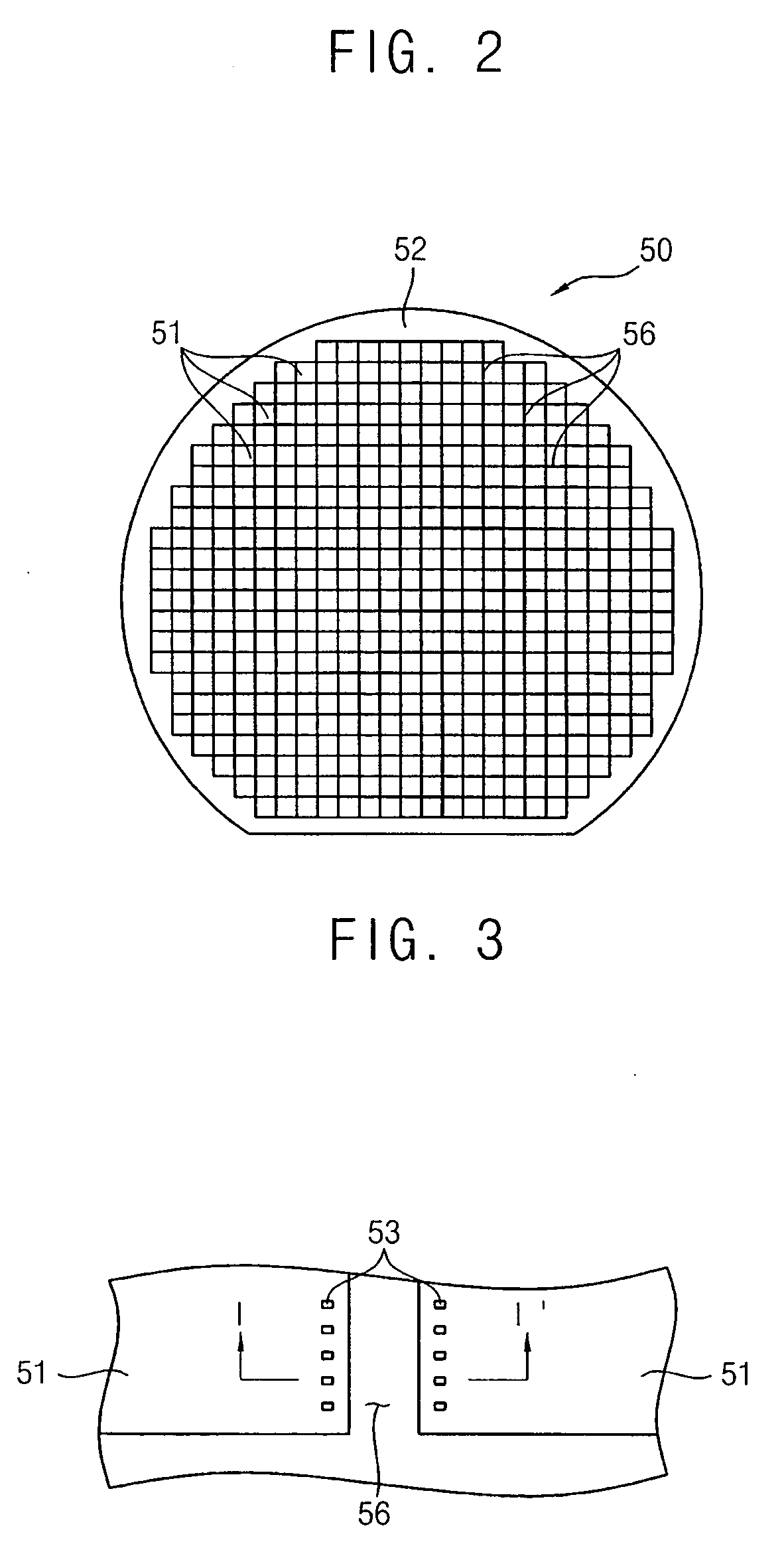
[0099] In a manner similar to the formation and dicing of the chips 51 from the common wafer 50, other chips can be formed and diced from another common wafer, in accordance with the second embodiment described above. For the purpose of the remainder of the present discussion, such other chips are referred to as first chips 21 that are formed and diced from a common first wafer 20, while chips 51 are referred to as second chips 51 that are formed and diced from a common second wafer 50.

[0100] Referring to FIG. 22, a bottom surface of a separated first chip 21 is applied to a top surface of a printed circuit board 10, or other package substrate. The printed circuit board 10 includes a plurality of chip bonding pads 14, or landing pads, that serve as an interconnect location for conductive paths on the printed circuit board 10. The bonding pads 14 include optional conductive pads 125 on an upper surface thereof. The conductive pads 125 comprise, for example, a low melting point materi...

third embodiment

[0105]FIGS. 24 through 29 are sectional views of a method for fabricating a stacked chip package, in accordance with the present invention.

[0106] In the first and second embodiments above, separated chips are individually aligned and stacked on a substrate to form chip stack packages in a manner that is consistent with a chip level bonding configuration. In the following third embodiment, entire wafers including multiple chips, or segments of such wafers including multiple chips, are aligned and stacked, and applied to a substrate, prior to dicing of the chips in a manner that is consistent with a wafer level bonding configuration.

[0107] Referring to FIG. 24, a second wafer 50 is prepared in a manner similar to that of FIGS. 4 through 12 above to include a patterned insulator layer 122 and patterned adhesive layer 123, the adhesive layer comprising, for example, a photosensitive polymer material, as described above. The photosensitive polymer adhesive layer 123 is partially cured, ...


PUM


Abstract

In a stacked chip configuration, and manufacturing methods thereof, the gap between a lower chip and an upper chip is filled completely using a relatively simple process that eliminates voids between the lower and upper chips and the cracking and delamination problems associated with voids. The present invention is applicable to both chip-level bonding and wafer-level bonding approaches. A photosensitive polymer layer is applied to a first chip, or wafer, prior to stacking the chips or stacking the wafers. The photosensitive polymer layer is partially cured, so that the photosensitive polymer layer is made to be structurally stable, while retaining its adhesive properties. The second chip, or wafer, is stacked, aligned, and bonded to the first chip, or wafer, and the photosensitive polymer layer is then cured to fully bond the first and second chips, or wafers. In this manner, adhesion between chips / wafers is greatly improved, while providing complete fill of the gap. In addition, mechanical reliability is improved and CTE mismatch is reduced, alleviating the problems associated with warping, cracking and delamination, and leading to an improvement in device yield and device reliability.

Description

RELATED APPLICATIONS [0001] This application claims priority under 35 U.S.C. 119 to Korean Patent Application No. 10-2005-0080655 filed on Aug. 31, 2005, the content of which is incorporated herein by reference in its entirety. This application is related to U.S. patent application Ser. No. ______, entitled “Stacked Chip Package Using Photosensitive Polymer and Manufacturing Method Thereof”, by Yong-Chai Kwon, et al., filed of even date herewith and commonly owned with the present application, the content of which is incorporated herein by reference, in its entirety. FIELD OF THE INVENTION [0002] The present invention relates to semiconductor device packages including a stacked chip package configuration that utilizes a photosensitive polymer including adhesive and warp prevention properties, and manufacturing methods thereof. BACKGROUND OF THE INVENTION [0003] Semiconductor manufacturing and packaging technology has evolved to the point where device packages can include multiple in...

Claims


Application Information

Patent Timeline
Patent Type & Authority Applications(United States)
IPC IPC(8): H01L23/48
CPCH01L21/76898H01L23/481H01L2924/0002H01L2224/0401H01L2924/0665H01L2924/014H01L2924/0105H01L2924/01033H01L2924/01024H01L2924/01006H01L24/11H01L24/12H01L24/16H01L24/31H01L24/83H01L24/90H01L24/94H01L25/0657H01L25/50H01L2221/68372H01L2224/02311H01L2224/02321H01L2224/0557H01L2224/13009H01L2224/13021H01L2224/13099H01L2224/16145H01L2224/83136H01L2224/83194H01L2224/838H01L2225/06513H01L2225/06524H01L2225/06541H01L2924/01013H01L2924/01022H01L2924/01029H01L2924/01046H01L2924/01073H01L2924/01075H01L2924/01079H01L2924/01082H01L2924/01322H01L2924/04953H01L2924/14H01L2224/16147H01L2224/16237H01L2224/81141H01L2224/2919H01L2924/01005H01L2924/00H01L2924/3512H01L2224/05552H01L24/02H01L24/13H01L2224/02372H01L2224/02379H01L2224/05568H01L2224/05571H01L2224/08112H01L2224/16148H01L2924/0001H01L2924/181H01L2224/02H01L23/12H01L23/48
Inventor KWON, YONG-CHAILEE, KANG-WOOKMA, KEUM-HEEHAN, SEONG-ILLEE, DONG-HO
Owner SAMSUNG ELECTRONICS CO LTD
Why Eureka
Try Eureka