Manufacture method for semiconductor device suitable for forming wirings by damascene method and semiconductor device

a manufacturing method and semiconductor technology, applied in semiconductor devices, semiconductor/solid-state device details, electrical equipment, etc., can solve the problems of insufficient adhesion of state before heat treatment, difficult to fill wiring trenches and via holes with copper at good reproductivity, etc., to prevent copper wiring from being peeled off, good reproductivity, and the effect of sufficient tight adhesion of wiring material

Active Publication Date: 2007-03-01
FUJITSU LTD
View PDF10 Cites 36 Cited by
  • Summary
  • Abstract
  • Description
  • Claims
  • Application Information

AI Technical Summary

Benefits of technology

[0015] It is expected that a copper wiring can be prevented from being peeled off, if heat treatment is executed to form a barrier layer of MnSiO compound before copper electroplating is performed. However, heat treatment is executed before copper electroplating, the seed layer of CuMn alloy is aggregated and it becomes difficult to fill a wiring trench and a via hole with copper at good reproductivity.
[001...

Problems solved by technology

It can be understood from this that the state before heat treatment does not retain sufficient tight adhesion.
However, heat treatment is executed before cop...

Method used


Image

  • Manufacture method for semiconductor device suitable for forming wirings by damascene method and semiconductor device
  • Manufacture method for semiconductor device suitable for forming wirings by damascene method and semiconductor device
  • Manufacture method for semiconductor device suitable for forming wirings by damascene method and semiconductor device

Examples


first embodiment

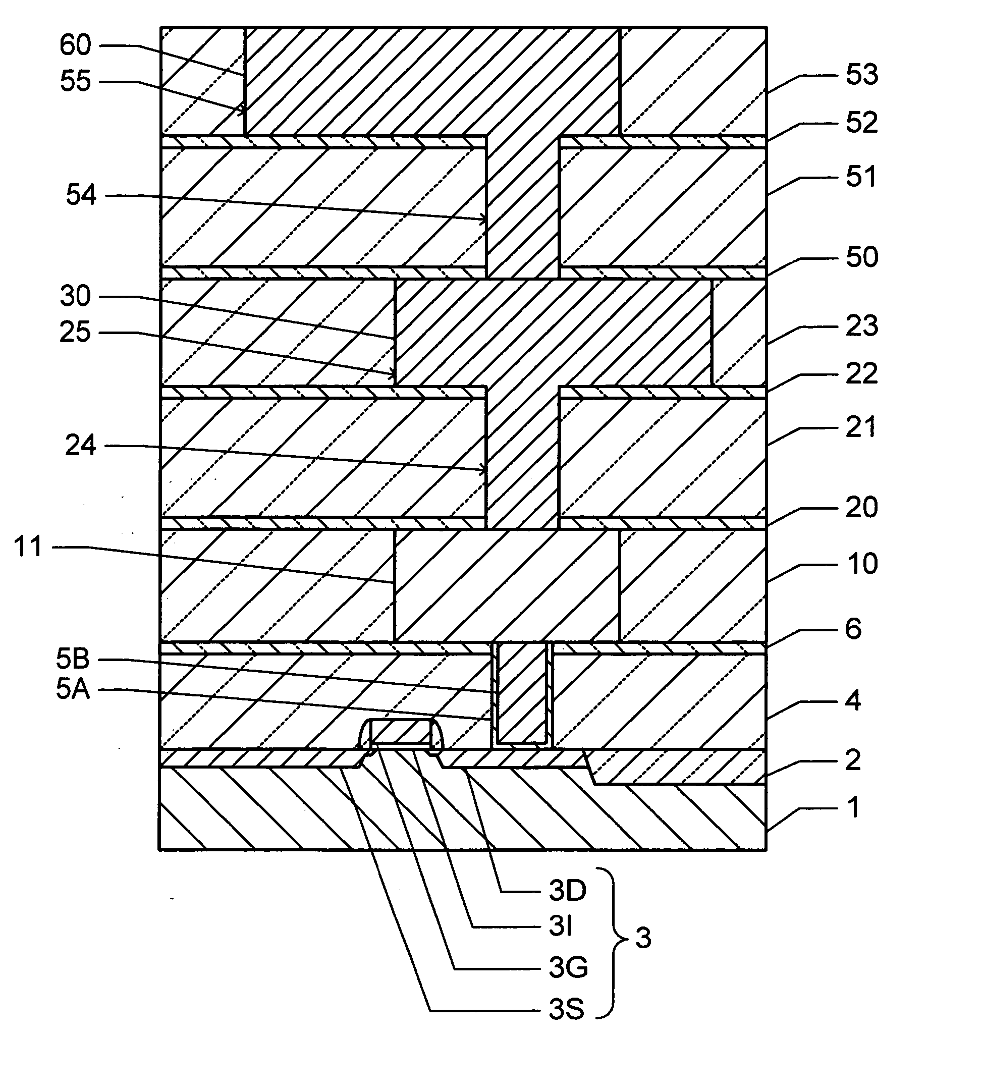
[0049] In the first embodiment described above, the barrier layer 34 prevents copper diffusion and enhances tight adhesion of the conductive member 33. Before the barrier layer 34 is formed, i.e., in the state shown in FIG. 2D, the adhesion layer 31 of Ag enhances tight adhesion of the auxiliary film 32 and conductive member 33. It is therefore possible to prevent peel-off of the conductive member 33.

[0050] Tight adhesion was evaluated by actually forming: 25 samples A having a CuMn alloy film of 90 nm in thickness formed on a silicon oxide (SiO2) film; 25 samples B having a CuMn alloy film of 90 nm in thickness and a silicon oxycarbide (SiOC) film; 25 samples C having an Ag film inserted between a CuMn alloy film of 90 nm in thickness and an SiO2 film; and 25 samples D having an Ag film inserted between a CuMn alloy film of 90 nm in thickness and an SiOC film. Tight adhesion was evaluated by JIS crosscut tape tests ASTM3359-87. In all 25 samples A and all 25 samples B, peel-off aro...

second embodiment

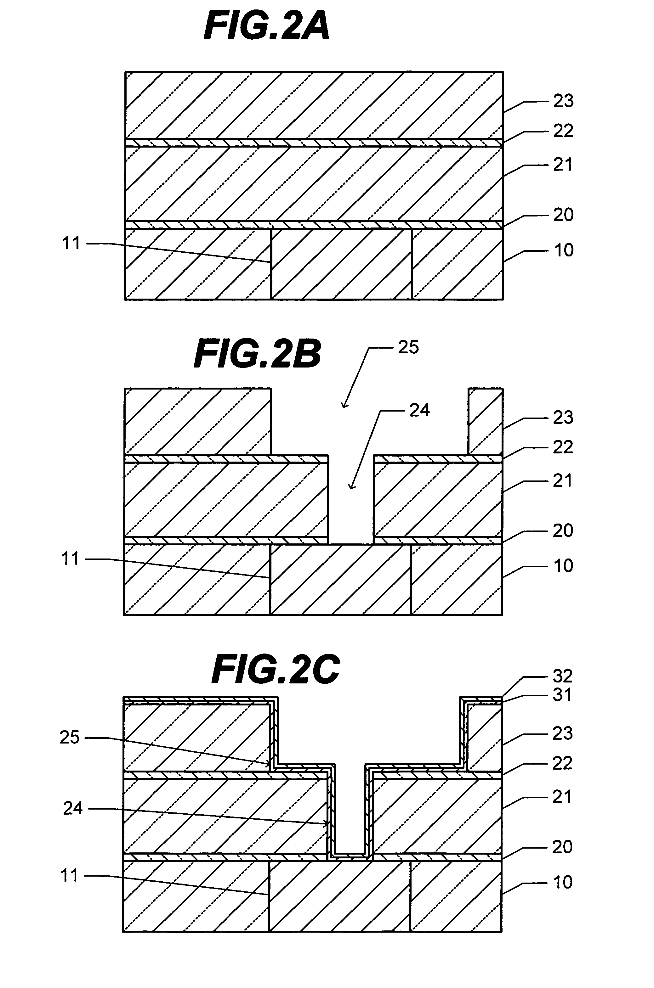
[0058] Next, a semiconductor device manufacture method will be described with reference to FIGS. 6A to 6C.

[0059] The processes of forming the wiring trench 25 and via hole 24 shown in FIG. 6A are the same as those of the first embodiment described with reference to FIGS. 2A and 2B. After the wiring trench 25 and via hole 24 are formed, the substrate is placed in a pre-processing chamber and the substrate surface is exposed to silane (SiH4) plasma. A reformed film 41 added with Si is formed in an upper surface layer of the interlayer insulating film23 and in inner surface layers of the wiring trench 25 and via hole 24. The reformed film 41 contains Si in higher concentration than a region remote from the surfaces of the interlayer insulating films 23 and 21.

[0060] An auxiliary film 42 of CuMn alloy is formed on the reformed film 41, and a conductive member 43 is formed by electroplating copper. The auxiliary film 42 and conductive film 43 are formed by the same method as that of fo...


PUM


Abstract

An interlayer insulating film having a concave portion is formed on a semiconductor substrate. A tight adhesion film is formed on the inner surface of the concave portion and the upper surface of the insulating film. The surface of the adhesion layer is covered with an auxiliary film made of Cu alloy containing a first metal element. A conductive member containing a second metal element other than the first metal element is embedded in the concave portion, and deposited on the auxiliary film. Heat treatment is performed to make atoms of the first metal element in the auxiliary film segregate on the inner surface of the concave portion. The adhesion layer contains an element for enhancing tight adhesion of the auxiliary film more than if the auxiliary film is deposited directly on a surface of the interlayer insulating film. During the period until the barrier layer having also the function of enhancing tight adhesion, it becomes possible to retain sufficient tight adhesion of a wiring member and prevent peel-off of the wiring member.

Description

CROSS REFERENCE TO RELATED APPLICATION [0001] This application is based on and claims priority of Japanese Patent Application No. 2005-297955 filed on Oct. 12, 2005, the entire contents of which are incorporated herein by reference. BACKGROUND OF THE INVENTION [0002] A) Field of the Invention [0003] The present invention relates to a semiconductor device manufacture method and a semiconductor device, and more particularly to a semiconductor device manufacture method suitable for forming wirings by filling concave portions formed in an interlayer insulating film with conductor and a semiconductor device. [0004] B) Description of the Related Art [0005] Miniaturization of wirings and increasing of wiring layers are progressing as semiconductor elements are highly integrated and chip sizes are reduced. In a logical element having a multi-layer wiring structure, a delay of a signal transmitting along a wiring is becoming a dominant factor of lowering an operation speed of the logical ele...

Claims


Application Information

Patent Timeline
IPC IPC(8): H01L23/52
CPCH01L23/53238H01L23/53295H01L2924/0002H01L2924/00H01L21/76831H01L21/76846H01L21/76855H01L21/76864H01L21/76867
Inventor KITADA, HIDEKIOHTSUKA, NOBUYUKISHIMIZU, NORIYOSHINAKAO, YOSHIYUKI
Owner FUJITSU LTD
Why Eureka
Try Eureka