Thin film led

a technology of leds and films, applied in the direction of discharge tubes/lamp details, discharge tubes luminescnet screens, electric discharge lamps, etc., can solve the problems of low luminous efficiency, low lifetime of incandescent bulbs, and inability to meet the needs of light uniformity, etc., to reduce or eliminate the degradation of led chips, led chip, lead and/or phosphor, and improve light uniformity

Inactive Publication Date: 2007-03-01
SUZHOU LEKIN SEMICON CO LTD
View PDF8 Cites 68 Cited by
  • Summary
  • Abstract
  • Description
  • Claims
  • Application Information

AI Technical Summary

Benefits of technology

[0019] The principles of the present invention provide for white-light LEDs and for methods of fabricating white-light LEDs. Embodiments of white-light LEDs that are in accord with the principles of the present invention have reduced or eliminated bonding wire, LED chip, lead, and / or phosphor degradation. Such white-light LEDs can be fabricated on-chip, with improved light uniformity, and in such a manner that the light output is not heavily dependent on the thickness of a substrate.

Problems solved by technology

However, conventional LEDs are relatively monochromatic light sources.
Unfortunately, some applications require white light, which includes all primary colors.
Although inexpensive, incandescent bulbs have fairly short lifetimes and low luminous efficiency.
While more efficient, fluorescent lamps also tend to have limited lifetimes. Furthermore, fluorescent lamps require relatively large, heavy and expensive support devices, such as voltage stabilizers.
However, blue LEDs have been relatively difficult to fabricate, primarily because of difficulties in fabricating high quality crystals having a suitable band gap.
While successful in producing white light, three-component (green, red and blue) LEDs have problems.
Additionally, three-component LEDs require careful balancing of optical outputs to achieve high quality white light, a balance that is difficult to maintained over time and temperature and that requires careful and expensive fabrication.
The necessity of optical balancing combined with a relatively complicated drive circuitry means that three-component LEDs are, in practice, difficult and expensive to fabricate.
Despite their numerous advantages, white-light emitting LEDs similar to the one shown in FIG. 1 have problems.
Another problem with white-light emitting LEDs similar to the one shown in FIG. 1 is that the hemispherical top 18 of the package 17 results in a “ring pattern” in the emitted light.
Thus, the emitted light has poor luminance uniformity.
The hemispherical top 18 also makes it difficult to reliably coat phosphors inside the package if such coating is required.
Another serious problem with white-light emitting LEDs similar to the one shown in FIG. 1 is that the actual production of white light does not come from the light-producing LED chip 14, which emits only blue light, but from phosphor 16 within the package 17.
This makes it difficult to form surface mounted devices.
While the techniques taught in U.S. Pat. No. 6,337,536 are generally successful, they have problems.
Furthermore, the materials used in U.S. Pat. No. 6,337,536 may not be optimal in specific applications.

Method used


Image

  • Thin film led
  • Thin film led
  • Thin film led

Examples


Embodiment Construction

[0038] The following generally describes a process for fabricating on-chip white LEDs. While that description is an advantageous method of fabricating white LEDs, the principles of the present invention are not limited to that described method. Accordingly, the present invention is to be limited only by the claims that follow as understood and interpreted according to United States Patent Laws.

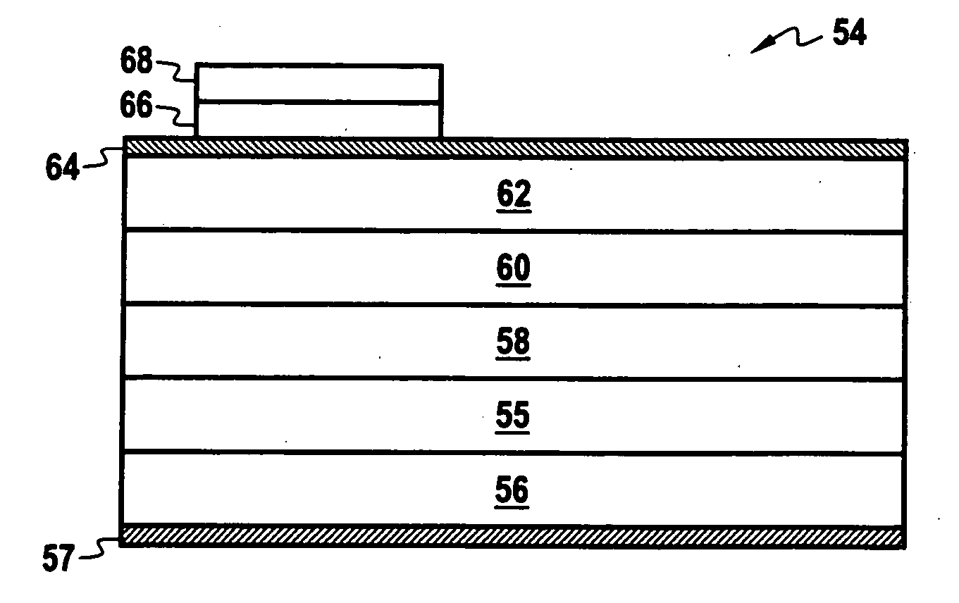
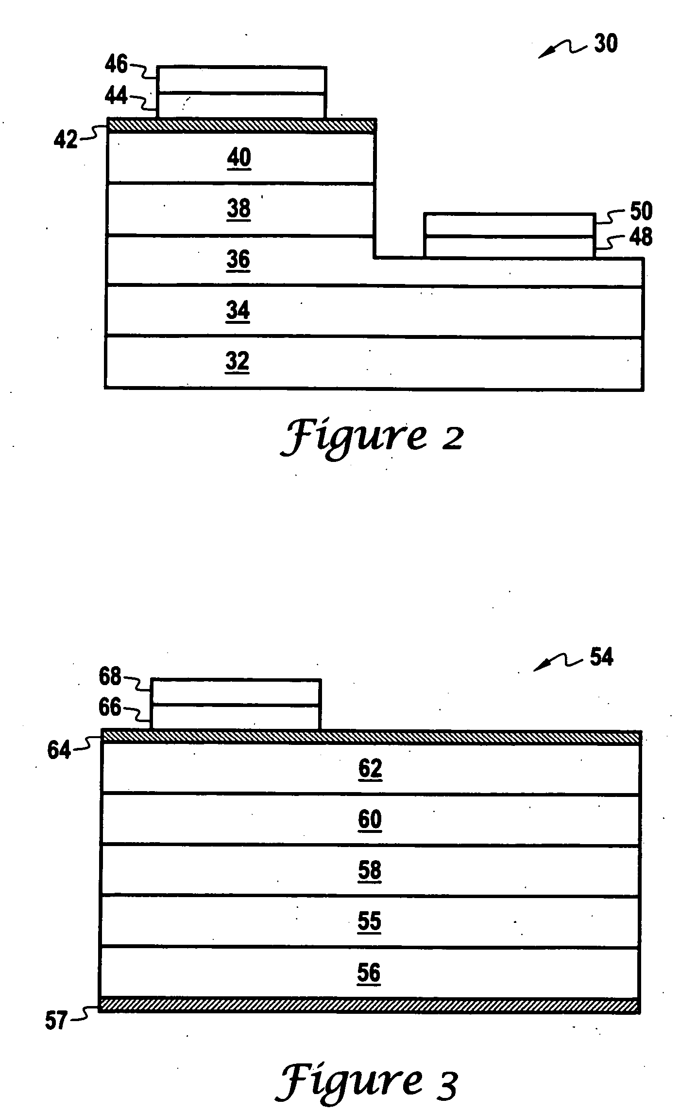
[0039] Fabrication of a white-light emitting diode that is in accord with the principles of the present invention begins with procurement of, such as by fabrication, a blue-LED chip having p and n contact pads. FIGS. 2 and 3 illustrate suitable blue-LED chips. In particular, FIG. 2 illustrates a lateral topology blue-LED chip 30 that is fabricated on a sapphire substrate 32. An n-GaN buffer layer 34 is formed on the substrate 32. A relatively thick n-GaN epitaxial layer 36 is then formed on the buffer layer 34. An active layer 38 having multiple quantum wells of aluminum-indium-gallium-nitrid...


PUM


Abstract

A method of fabricating a light emitting diode (LED) includes providing an LED chip that emits light having a first wavelength where the LED chip includes a first electrical contact and a second electrical contact. The method further includes forming a tinted thin film layer over the LED chip where the tinted thin film layer interacts with the first wavelength light to produce a light having a second wavelength.

Description

[0001] This patent application is a divisional of patent application Ser. No. 10 / 795,287 filed Mar. 9, 2004, which in turn is a continuation of patent application Ser. No. 10 / 316,004 filed Dec. 11, 2002, both of which are incorporated herein by reference.BACKGROUND OF THE INVENTION [0002] 1. Field of the Invention [0003] The present invention relates to light emitting diodes (LEDs). More particularly, this invention relates to light emitting LEDs having active layers that produce light at one wavelength, but that emit light at another wavelength. [0004] 2. Discussion of the Related Art [0005] Light emitting diodes (“LEDs”) are well-known semiconductor devices that convert electrical current into light. An LED produces light by exciting electrons across the band gap between a conduction band and a valence band of a semiconductive active (light-emitting) layer. That electron transition generates light at a wavelength (color) that depends on the band gap. Thus, the color of the light (...

Claims


Application Information

Patent Timeline
Patent Type & Authority Applications(United States)
IPC IPC(8): H01L21/00H01L33/50H05B33/14
CPCH01L33/44H01L33/508H01L33/507H01L2224/48091H01L2224/48247H01L2224/48257H01L2224/48465H01L2224/49107H01L2224/4918H01L2924/181
Inventor JEON, HYEONG TAG
Owner SUZHOU LEKIN SEMICON CO LTD
Why Eureka
Try Eureka