Method and apparatus for improving nitrogen profile during plasma nitridation

a plasma nitridation and nitrogen profile technology, applied in the direction of electrical apparatus, basic electric elements, electric discharge tubes, etc., can solve the problems of reducing the boron penetration of the gate dielectric to the silicon channel, deteriorating the interfacial properties, and reducing the nitridation rate of conventional high density plasma nitridation sources,

Inactive Publication Date: 2007-03-01
FREESCALE SEMICON INC
View PDF28 Cites 71 Cited by
  • Summary
  • Abstract
  • Description
  • Claims
  • Application Information

AI Technical Summary

Problems solved by technology

In addition, nitrogen in the gate dielectric reduces boron penetration to the silicon channel during ion implantation.
Although thin films can be readily nitrided using thermal means, one major concern with thermal nitridation techniques is that there is considerable amount of nitrogen present near the dielectric/silicon interface, which deteriorates the interfacial properties.
Wh...

Method used


Image

  • Method and apparatus for improving nitrogen profile during plasma nitridation
  • Method and apparatus for improving nitrogen profile during plasma nitridation
  • Method and apparatus for improving nitrogen profile during plasma nitridation

Examples


Embodiment Construction

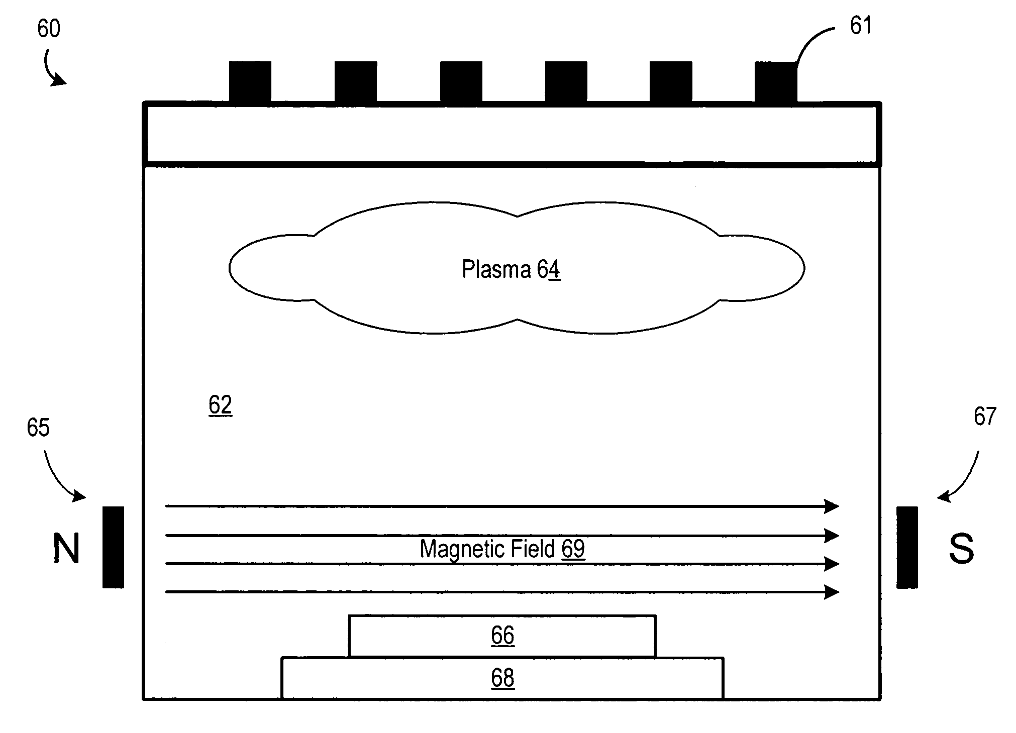
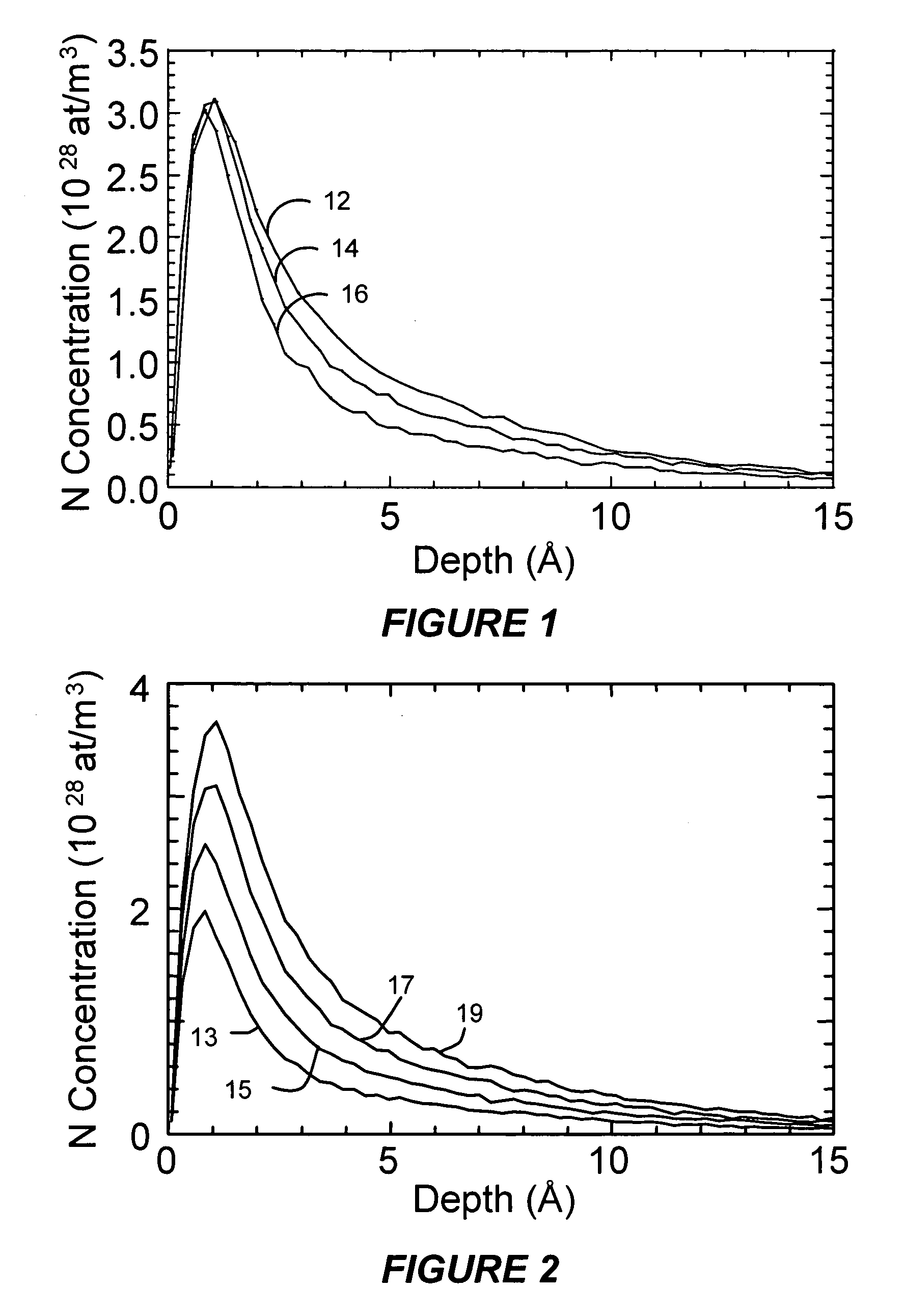
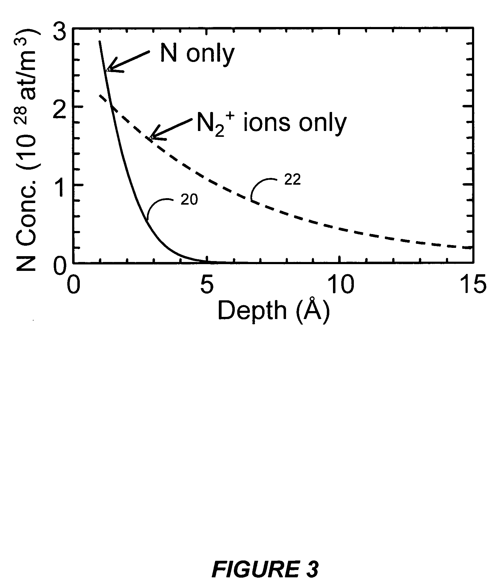
[0017] A method and apparatus are described for blocking, filtering or otherwise removing nitrogen ions from a plasma nitridation source so that only atomic nitrogen is absorbed into the surface of a dielectric film. The disclosed techniques may be used to fabricate a semiconductor device having a dielectric layer, such as a gate dielectric in a field effect transistor or a non-volatile memory device or a dielectric in a capacitor. The improved performance resulting from such a process may advantageously be incorporated with CMOS process technology. Various illustrative embodiments of the present invention will now be described in detail with reference to the accompanying figures. While various details are set forth in the following description, it will be appreciated that the present invention may be practiced without these specific details, and that numerous implementation-specific decisions may be made to the invention described herein to achieve the device designer's specific go...


PUM


Abstract

A semiconductor manufacturing apparatus and process for forming a nitrided dielectric film includes generating a plasma source (44) over a wafer structure (46), where the plasma source (44) includes neutral species (such as nitrogen atoms) and charged species (such as nitrogen ions) that are formed in an inductively coupled plasma reactor. Before the charged species in the plasma (44) can penetrate the wafer structure (46), an electrically connected mesh structure (45, 47) between the plasma source (44) and wafer structure (46) blocks the charged species. In addition or in the alternative, a magnetic field (69) aligned in parallel with the surface of the wafer structure (66) is established in close proximity to the wafer structure (66) in order to trap the charged species. By removing charged species, an improved, narrower nitrogen concentration profile is obtained.

Description

BACKGROUND OF THE INVENTION [0001] 1. Field of the Invention [0002] The present invention is directed in general to the field of semiconductor devices. In one aspect, the present invention relates to the formation a dielectric layer. [0003] 2. Description of the Related Art [0004] When transistor gate dielectric layers incorporate nitrogen, the transistor's electrical characteristics (leakage current, short channel effects) are improved since the nitridation increases the dielectric constant, thereby allowing use of thicker films. In addition, nitrogen in the gate dielectric reduces boron penetration to the silicon channel during ion implantation. Early nitridation experiments used thermal techniques to expose dielectric films to various nitrogen containing gases (NO, N2O, NH3, N2) at elevated temperatures. Although thin films can be readily nitrided using thermal means, one major concern with thermal nitridation techniques is that there is considerable amount of nitrogen present ne...

Claims


Application Information

Patent Timeline
IPC IPC(8): H01L21/31
CPCH01J37/3266H01L21/3144H01L21/28185H01J2237/3387H01L21/02247H01L21/02252
Inventor RAUF, SHAHIDVENTZEK, PETER L.G.
Owner FREESCALE SEMICON INC
Why Eureka
Try Eureka