Organic electroluminescence device

a technology of electroluminescent devices and organic materials, which is applied in the direction of discharge tube luminescnet screens, other domestic articles, natural mineral layered products, etc., can solve the problems of compound of patent document 1 not achieving satisfactory luminous efficiency, and achieve the effects of reducing different interactions between organic layers, high efficiency, and long li

Active Publication Date: 2007-03-08
IDEMITSU KOSAN CO LTD
View PDF4 Cites 45 Cited by
  • Summary
  • Abstract
  • Description
  • Claims
  • Application Information

AI Technical Summary

Benefits of technology

[0011] According to the invention, an organic EL device can be provided which is driven at a low voltage and exhibits a high efficiency and a long lifetime.
[0012] In more detail, since different interactions between the organic layers can be reduced by introducing a common molecular group into the first layer, the emitting layer, and the second layer, a carrier mobility barrier between each organic layer can be reduced. Therefore, the device can be driven at a significantly reduced voltage, whereby a highly efficient device can be obtained.

Problems solved by technology

However, the compound of the patent document 1 does not achieve a satisfactory luminous efficiency.

Method used


Image

  • Organic electroluminescence device
  • Organic electroluminescence device
  • Organic electroluminescence device

Examples


example 1

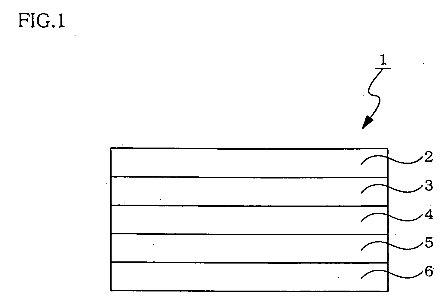
[0081] A glass substrate with an ITO transparent electrode (25 mm×75 mm×0.7 mm) was subjected to ultrasonic cleaning in isopropyl alcohol for five minutes and then subjected to UV ozone cleaning for 30 minutes. The cleaned glass substrate with the transparent electrode was installed in a substrate holder of a vacuum deposition device, and a TCTA film with a thickness of 95 nm was formed on the surface of the glass substrate on which the transparent electrode was formed so that the transparent electrode was covered with the TCTA film. The TCTA film functions as a hole transporting layer. The compound (A) was deposited on the TCTA film as a host compound to a thickness of 30 nm to form an emitting layer. The Ir metal complex compound (B) was added as a phosphorescent Ir metal complex dopant. The concentration of the metal complex compound (B) in the emitting layer was adjusted to 7.5 wt %. This film functions as an emitting layer. The compound (C) was formed on this film to a thicknes...

example 2

[0083] An organic EL device was fabricated in the same manner as in Example 1 except for using the compound (D) instead of the compound (B). After sealing the resulting device, electricity was supplied to the device in the same manner as in Example 1.

[0084] Blue green light with a luminance of 113 cd / m2 was obtained at a voltage of 5.5 V and a current density of 0.35 mA / cm2. The luminous efficiency was 32 cd / A. The device was driven at a constant current and an initial luminance of 200 cd / m2. The period of time until the luminance was halved to 100 cd / m2 was measured and found to be 730 hours.

example 3

[0085] An organic EL device was fabricated in the same manner as in Example 1 except for using the compound (E) instead of the compound (B). After sealing the resulting device, electricity was supplied to the device in the same manner as in Example 1.

[0086] Green light with a luminance of 108 cd / m2 was obtained at a voltage of 5.5 V and a current density of 0.14 mA / cm2. The luminous efficiency was 77 cd / A and 44 lm / W. The device was driven at a constant current and an initial luminance of 1500 cd / m2. The period of time until the luminance was halved to 750 cd / m2 was measured and found to be 3210 hours.


PUM

PropertyMeasurementUnit
singlet energy levelaaaaaaaaaa
triplet energy levelaaaaaaaaaa

Abstract

An organic electroluminescent device (1) including an anode (2), a cathode (6), and at least a first layer (3), a second layer (4), and a third layer (5) provided between the anode (2) and the cathode (6) in that order from the anode side. At least one of the first to third layers (3), (4), and (5) includes a phosphorescent compound. At least one of the first to third layers (3), (4), and (5) is an emitting layer. At least three compounds respectively forming the first layer (3), the second layer (4), and the third layer (5) other than the phosphorescent compound are compounds of the following formula (1).
wherein R1 to R7 each represent a hydrogen atom or a substituent, provided that adjacent substituents may form a ring.

Description

BACKGROUND OF THE INVENTION [0001] 1. Field of the Invention [0002] The invention relates to an organic electroluminescent device. In particular, the invention relates to a phosphorescent organic electroluminescent device. [0003] 2. Description of Related Art [0004] An organic electroluminescent device (organic EL device) using an organic material is a promising solid-state emitting type inexpensive and large full-color display device, and has been extensively developed. [0005] In general, when an electric field is applied between electrodes of an organic EL device, electrons are injected from the cathode and holes are injected from the anode. The electrons recombine with the holes in the emitting layer to produce an excited state, and the energy is emitted as light when the excited state returns to the ground state. [0006] An organic EL device includes an emitting layer, a pair of opposing electrodes positioned on either side of the emitting layer, and a layer which transports hole...

Claims


Application Information

Patent Timeline
Patent Type & Authority Applications(United States)
IPC IPC(8): H01L51/54
CPCH01L51/0059H01L51/0072Y10S428/917H01L51/5016H01L51/0086H10K85/631H10K85/344H10K85/6572H10K50/11H10K2101/10C09K11/06
Inventor IWAKUMA, TOSHIHIROMATSUURA, MASAHIDENAGASHIMA, HIDEAKIIKEDA, HIDETSUGUNAKAMURA, HIROAKIKUSUMOTO, TADASHI
Owner IDEMITSU KOSAN CO LTD
Why Eureka
Try Eureka