Clock generation circuit and clock generation method

Active Publication Date: 2007-03-15
MONTEREY RES LLC
View PDF4 Cites 7 Cited by
  • Summary
  • Abstract
  • Description
  • Claims
  • Application Information

AI Technical Summary

Benefits of technology

[0013] Now, there will be given an explanation on the case where the delay clocks are generated for the divided reference clock in the first delay circuit. The reference clock and the divided reference clock are coincident to each other in terms of phase, and the cycle of the divided reference clock is greater than that of the reference clock. Therefore, based on the reference clock, a specified time period within the cycle of the divided reference clock can be designated without fail. More specifically, in the selector circuit, a time period during which the signal levels of the divided reference clock signal and the delay clock signal are stable is designated based on the reference clock and the clock selecting operation is performed according to a modulation signal during the designated time period. Thereby, spi

Problems solved by technology

In this modulation, if the switching is done in a region where a signal level in the vicinity of the rising edge or falling edge of a delay clock signal is unstable, spike noise is generated.
If the switching is done with a timing intermediate between the timing of generation of a transition edge of a delay clock signal before switching and the timing of generation of a transition edge of the delay clock signal after switching, these transition edges are output so that a ha

Method used


Image

  • Clock generation circuit and clock generation method
  • Clock generation circuit and clock generation method
  • Clock generation circuit and clock generation method

Examples


first embodiment

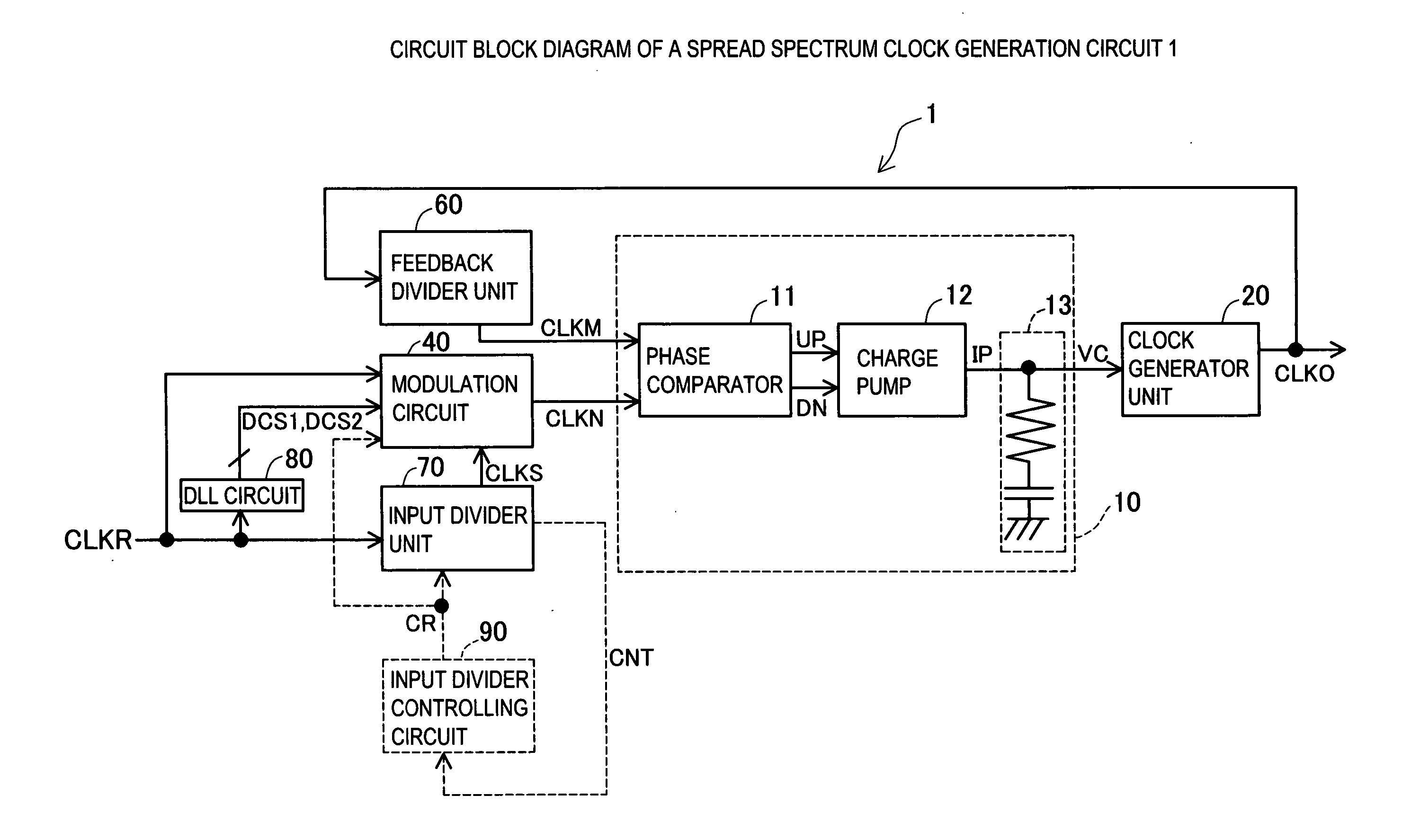
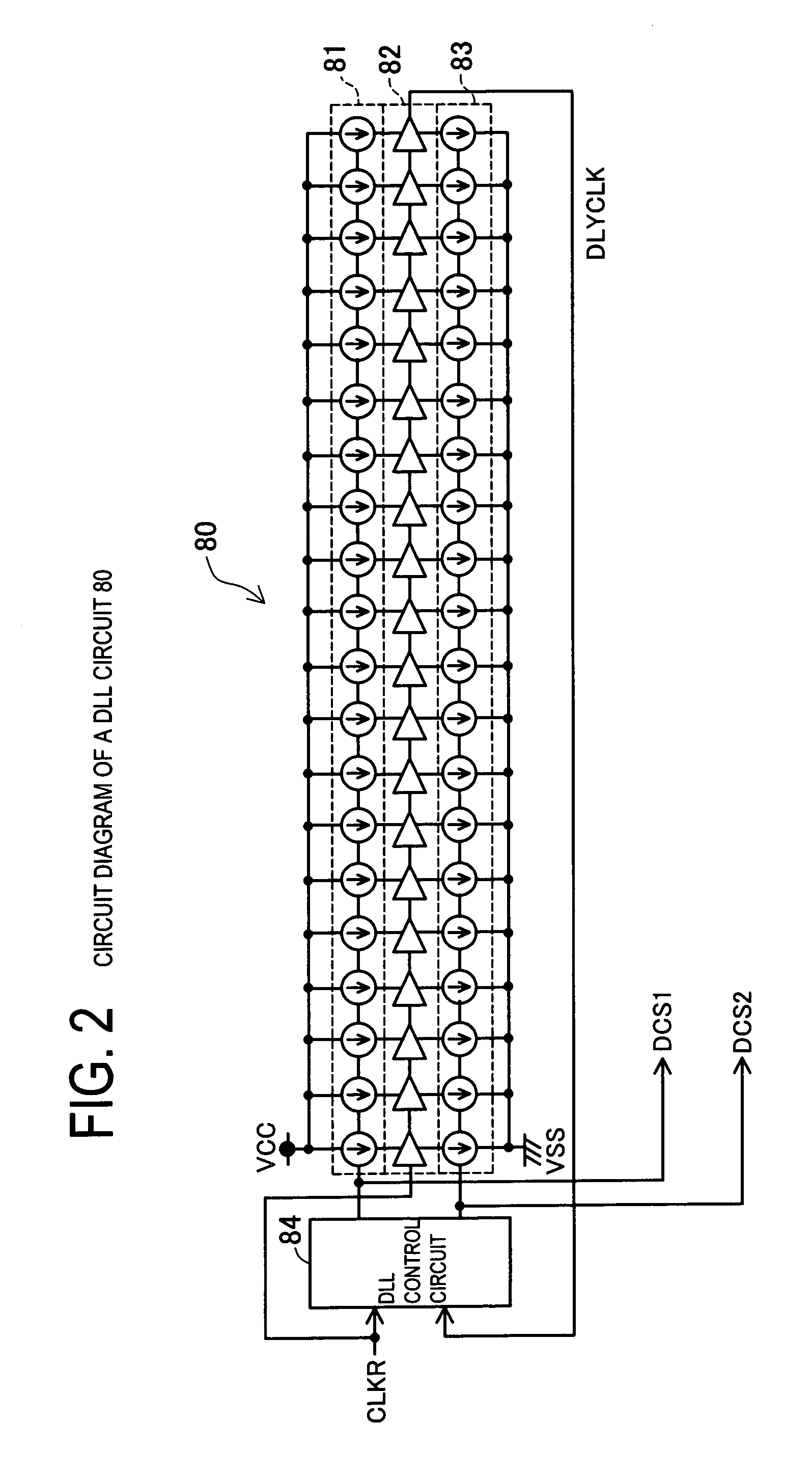
[0031] Next, reference will be made to FIGS. 4 to 6 to describe the operation of the spread spectrum clock generation circuit 1. The operation of the DLL circuit 80 will be explained. The delay circuit 82 delays the input clock signal CLKR and outputs the delay clock signal DLYCLK from the buffer of the last stage. The DLL control circuit 84 compares the phase of the input clock signal CLKR with the phase of the delay clock signal DLYCLK and controls the current values of the first current source unit 81 and the second current source unit 83 so as to make the phase difference between them equal to one cycle T0 (40 (ns)) of the input clock signal CLKR. That is, the DLL circuit 80 operates to make an adjustment so as to delay the phase of the delay clock signal DLYCLK from the input clock signal CLKR by one cycle T0. Thereby, the delay time for the buffer in each stage of the delay circuit 82 is made equal to the value obtained by dividing the cycle T0 by the number of buffer stages. ...

second embodiment

[0059] As fully described hereinabove, the spread spectrum clock generation circuit uses, for modulating the divided input clock signal CLKS, the first means for directly changing the cycle T1 of the divided input clock signal CLKS by changing the reload value CR of the input divider unit 70 and the second means for changing the cycle by sequentially selecting the delay clock signals CLKD1 to CLKD4 which are delayed from the divided input clock signal CLKS.

[0060] The minimum time of the modulation width obtained by the first means is equal to the cycle T0 (25 (ns)) of the input clock signal CLKR and therefore is sufficiently greater compared to the reference delay time tr=5 (ns) that is the minimum time of the modulation width obtained by the second means. Therefore, the modulation width can be arbitrarily set in increments of 5 (ns) through coarse adjustment of the modulation width in increments of 25 (ns) with the first means and fine adjustment of it in increments of 5 (ns) with...


PUM


Abstract

A clock generation circuit and a clock generation method are provided, which are capable of spread spectrum clock generation and accurate phase control of a reference clock signal and an output clock signal. To this end, an input divider unit 70 divides an input clock signal CLKR by 50 to output a divided input clock signal CLKS. A DLL circuit 80 operates to obtain delay control signals DCS1, DCS2. A modulation circuit 40 modulates, in response to the delay control signals DCS1, DCS2 and a modulation signal MOD output from a modulation control circuit 50, the divided input clock signal CLKS to output a modulation clock signal CLKN. A phase comparator 11 detects the phase difference between the modulation clock signal CLKN and a divided inner clock signal CLKM. A clock generation unit 20 generates an output clock signal CLKO having frequency corresponding to a phase difference signal from the phase comparator 11.

Description

CROSS-REFERENCE TO RELATED APPLICATIONS [0001] This application is based upon and claims the benefit of priority from the prior Japanese Patent Application No. 2005-268332 filed on Sep. 15, 2005, the entire contents of which are incorporated herein by reference. BACKGROUND OF THE INVENTION [0002] 1. Field of the Invention [0003] The present invention relates to a clock generation circuit. More particularly, the present invention relates to a clock generation circuit and a controlling method thereof, the clock generation circuit performing frequency modulation for spread spectrum by accurately controlling the phase difference between a reference clock signal and an output clock signal. [0004] 2. Description of Related Art [0005] In recent years, spread spectrum clock generators (abbreviated as SSCG) capable of reducing EMI (Electromagnetic Interference) noise have been receiving attention. SSCGs have a PLL circuit and perform frequency modulation while locking the frequency of an out...

Claims


Application Information

Patent Timeline
IPC IPC(8): H03L7/06G06F1/04H03C3/00H03K5/13H03L7/08H03L7/081H03L7/18
CPCH03L7/07H03L7/0812H03L7/081H03L7/0805H03L7/0818
Inventor MIYAZAKI, YUKISATO
Owner MONTEREY RES LLC
Why Eureka
Try Eureka