Solid-state imaging device, manufacturing method for solid-state imaging device, and camera using the same

a manufacturing method and imaging device technology, applied in the field can solve the problems of reducing the size of pigment particles, reducing the resolution and wavelength sensitivity, and increasing noise, so as to reduce the distance between the light shielding film and the light-receiving element, reduce the manufacturing method of solid-state imaging devices, and prevent color mixing

Inactive Publication Date: 2007-03-15
PANASONIC CORP
View PDF2 Cites 45 Cited by
  • Summary
  • Abstract
  • Description
  • Claims
  • Application Information

AI Technical Summary

Benefits of technology

[0052] Since the wavelength-selecting layer is constructed from inorganic materials, it can be formed using a process at some point during the semiconductor manufacturing process. Consequently, manufacture of the solid-state imaging device can be simplified.
[0053] Moreover, since the wavelength selecting layer is constructed from a multilayer film, the layer that selects wavelength can be made thinner and the distance between the light shielding film and the light-receiving elements reduced. Consequently, color mixing can be prevented and the amount of collected light increased.
[0054] The solid-state imaging device of the present invention includes a wavelength-selecting layer constructed from photonic crystal that selects the wavelengths of light that are to enter the corresponding light-receiving elements, which are two-dimensionally arranged in the semi-conductor substrate. As the wavelength-selecting layer is characterized by being constructed from photonic crystal, even when oblique light enters the wavelength-selecting layer of one of the pixels, light within the specified range of wavelengths is conducted vertically by the photonic crystal to the light-receiving elements, and other light is stopped. Consequently, light entering the color filter of one pixel does not enter any of the color filter sections of adjacent pixels, and color mixing can largely be prevented.
[0055] Here, the present invention includes a camera having the above-described solid-state imaging device. When a camera having the above-described characteristics is used, high quality images exhibiting very low levels of color mixing are obtained.
[0056] In the solid state imaging device manufacturing method of the present invention, in the manufacturing process to form, above the optoelectronic conversion units, the dielectric multilayer film that splits incident light according to wavelength, the method for sectionally varying the thickness of the insulation layer in order to realize the color splitting function makes use of a film forming process that effectively generates variations in the film thickness as the film is formed, rather than dry etching or wet etching to vary a thickness of a film that has already been formed. This enables better control of the film thickness, and reduction in unevenness in the film.
[0057] The above-described solid-state imaging devices have the dielectric multilayer film above the photoelectric converting unit in order to separate incident light according to wavelength. Here, the color separation can be realized by a single dielectric layer, included in the dielectric multilayer film, whose thickness varies between sections. This means that color separation can be realized using the dielectric multilayer film having a thickness substantially equivalent to the wavelength of incident light (approximately 500 nm). As a result, the color filter can be made thinner, and it is possible to significantly reduce the degradation of the color separation function caused by oblique light.

Problems solved by technology

With light entering a solid-state imaging device from various directions, there is a risk of the light that enters obliquely (hereinafter oblique light) being received by a light-receiving element other than the intended light-receiving element, thereby degrading color separation, decreasing resolution and wavelength sensitivity, and increasing noise.
However, there is a limit as to how far the size of the pigment particles can be reduced, beyond which a loss of sensitivity and color uniformity inevitably occurs.

Method used


Image

  • Solid-state imaging device, manufacturing method for solid-state imaging device, and camera using the same
  • Solid-state imaging device, manufacturing method for solid-state imaging device, and camera using the same
  • Solid-state imaging device, manufacturing method for solid-state imaging device, and camera using the same

Examples


first embodiment

[0089] (1) First Embodiment

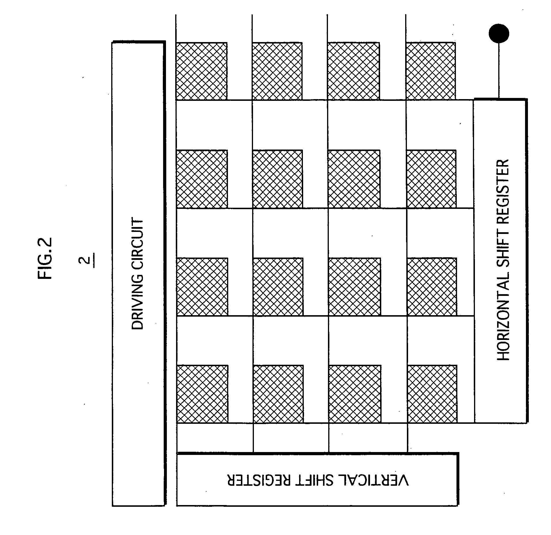
[0090]FIG. 2 is a plan view illustrating the construction of the solid-state imaging device of the first embodiment. As shown in FIG. 2, in the solid-state imaging device of the first embodiment, unit pixels (shaded parts), which are light-receiving units, are two-dimensionally arranged. A vertical shift register selects a row, and a horizontal shift register selects a signal in a pixel in the selected row. In this way, a color signal corresponding to each pixel is output through an output amplifier (not illustrated). A driving circuit causes the vertical shift register, horizontal shift register, and output amplifier to operate.

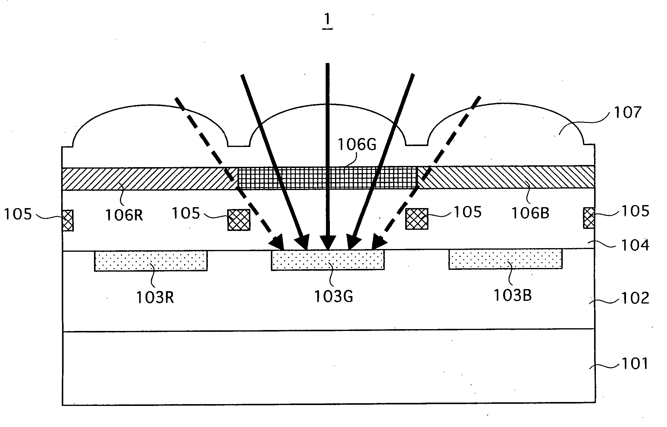
[0091]FIG. 3 is a cross -sectional view illustrating the construction of a solid-state imaging device 2 of the first embodiment of the present invention. Specifically, it shows three neighboring pixels in cross-section. As shown in FIG. 3, the solid-state imaging device 2 includes an N-type semiconductor substrate 201, a P-type se...

second embodiment

[0096] [2] Second Embodiment

[0097] The following describes the second embodiment of the present invention. The solid-state imaging device of the second embodiment largely resembles that of the first embodiment, but differs in that the color filter is composed of photonic crystals.

[0098] Photonic crystals are microstructures in which materials of differing permittivities and refraction indices, such as the semiconductor substrate and air for instance, are arranged in alternating layers, such that two contacting layers have a thickness of the order of the wavelength of light. Besides functioning as a filter that transmits only light of a specific wavelength, photonic crystals have the property of conducting incident light in a specific direction. Photonic crystals that do not transmit light of the particular range of wavelengths corresponding to the width of their band gap, namely photonic crystals having a photonic band gap are introduced in the following document:

[0099] NODA Susum...

third embodiment

[0101] [3] Third Embodiment

[0102] The following describes the third embodiment of the present invention. The solid-state imaging device of the third embodiment largely resembles that of the second embodiment, but differs in the positioning of the shielding film.

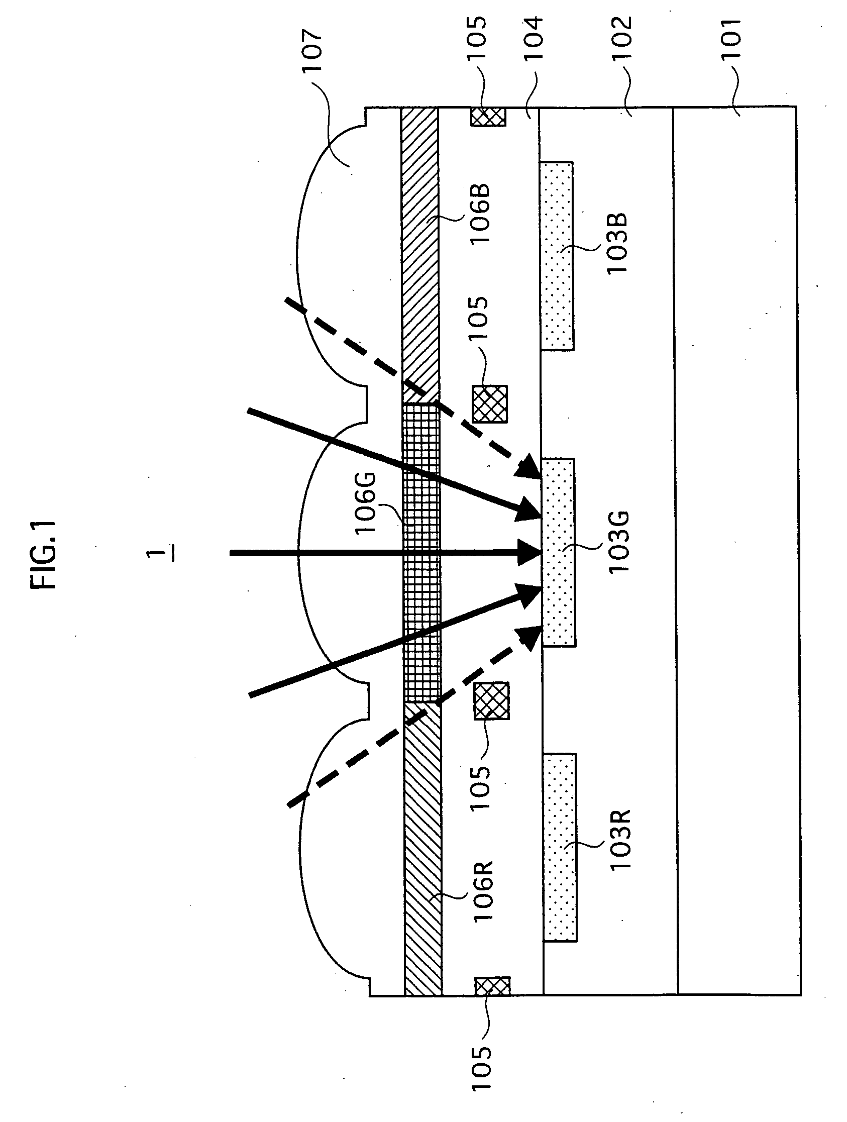
[0103]FIG. 4 is a cross-sectional view illustrating the construction of a solid-state imaging device of the third embodiment. As shown in FIG. 4, the solid-state imaging device 3 includes an N-type semiconductor substrate 301, a P-type semiconductor layer 302, light-receiving elements 303R, 303G, and 303B, insulation layers 304 and 307, a light shielding film 305, color filter 306R, 306G and 306B, and micro lenses 308.

[0104] The solid-state imaging device 3 is structured such that the P-type semiconductor substrate 302, the light-receiving elements 303R, 303G, and 303B, the light-transmitting insulating layer 304, the light shielding film 305, the color filter 306R, 306G, 306B, and the micro lenses 308 form respective layer...


PUM


Abstract

A solid-state imaging device includes a plurality of light-receiving units two-dimensionally arrayed in a semiconductor substrate, a filter unit operable to transmit incident lights of selected wavelengths to the plurality of light receiving units and a light shielding unit operable to shield incident light, the light shielding unit having a plurality of apertures, each aperture opposing a corresponding light receiving unit. Here, on a path of incident light from the light shielding unit to the plurality of light shielding units, the filter unit is disposed between the light shielding unit and the plurality of light-receiving units. The solid-state imaging device prevents color mixing caused by oblique light.

Description

TECHNICAL FIELD [0001] The present invention relates to a solid-state imaging device, a manufacturing method for a solid-state imaging device, and a camera using the same, and in particular to a technique for achieving a color solid-state imaging device of improved performance and smaller size. BACKGROUND ART [0002] In solid-state imaging devices, light receiving elements corresponding to red (R), green (G), and blue (B) are arranged, for example, in a Bayer array. FIG. 1 is a schematic cross-sectional view illustrating a construction of a conventional solid-state imaging device. As shown in FIG.1, a solid-state imaging device 1 includes an N-type semi-conductor layer 101, a P-type semiconductor layer 102, light receiving elements 103R, 103G, 103B, an insulation layer 104, light shielding films 105, color filter 106R, 106G, and 106B, and collective lenses 107. [0003] The P-type semiconductor layer 102 is formed on the N-type semiconductor layer 101. The light-receiving elements 103R...

Claims


Application Information

Patent Timeline
Patent Type & Authority Applications(United States)
IPC IPC(8): H04N9/04H01L31/0216H01L31/0232H04N5/225
CPCH01L27/14621H01L27/14627H01L31/0232H01L31/02162H01L31/02164H01L27/14685H01L31/02327
Inventor YAMAGUCHI, TAKUMIKASUGA, SHIGETAKAMURATA, TAKAHIKOORITA, KENJI
Owner PANASONIC CORP
Why Eureka
Try Eureka