A metal fuse for semiconductor devices and methods of manufacturing thereof

Inactive Publication Date: 2007-03-22
TAIWAN SEMICON MFG CO LTD
View PDF10 Cites 7 Cited by
  • Summary
  • Abstract
  • Description
  • Claims
  • Application Information

AI Technical Summary

Benefits of technology

[0004] Described is a metal fuse in a semiconductor device that can be readily blown without compromising device reliability and methods of manufacturing thereof. Integrated circuits are initially formed on a semiconductor substrate, where the integrated circuits can include multiple interconnect layers. Metal fuses are subsequently formed over the interconnect layers. A polymeric layer is then formed over the metal fuses. The polymeric coating allows an external radiation source to penetrate and “blow up” the underlying metal fuses with less energy than typically required by conventional techniques. As a result, when less energy is used, the likelihood of damaging other circuit components decreases, while th

Problems solved by technology

As a result, when less energy is used, the likelihood of damaging other circuit component

Method used


Image

  • A metal fuse for semiconductor devices and methods of manufacturing thereof
  • A metal fuse for semiconductor devices and methods of manufacturing thereof
  • A metal fuse for semiconductor devices and methods of manufacturing thereof

Examples


Embodiment Construction

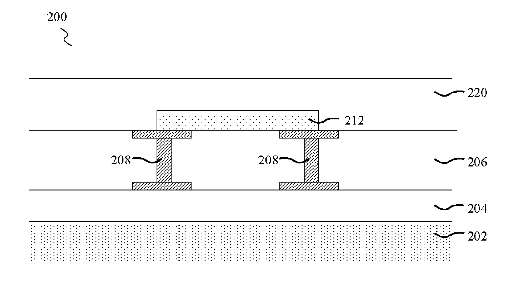
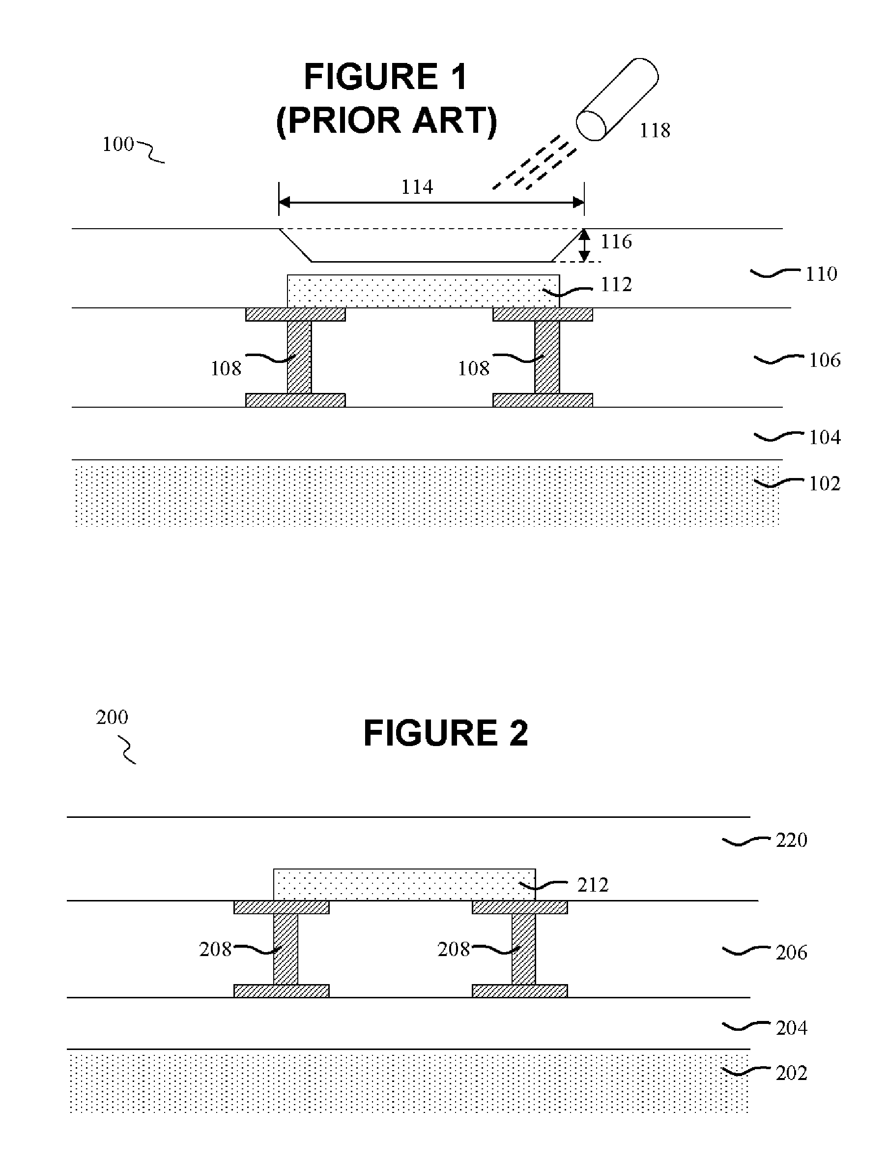
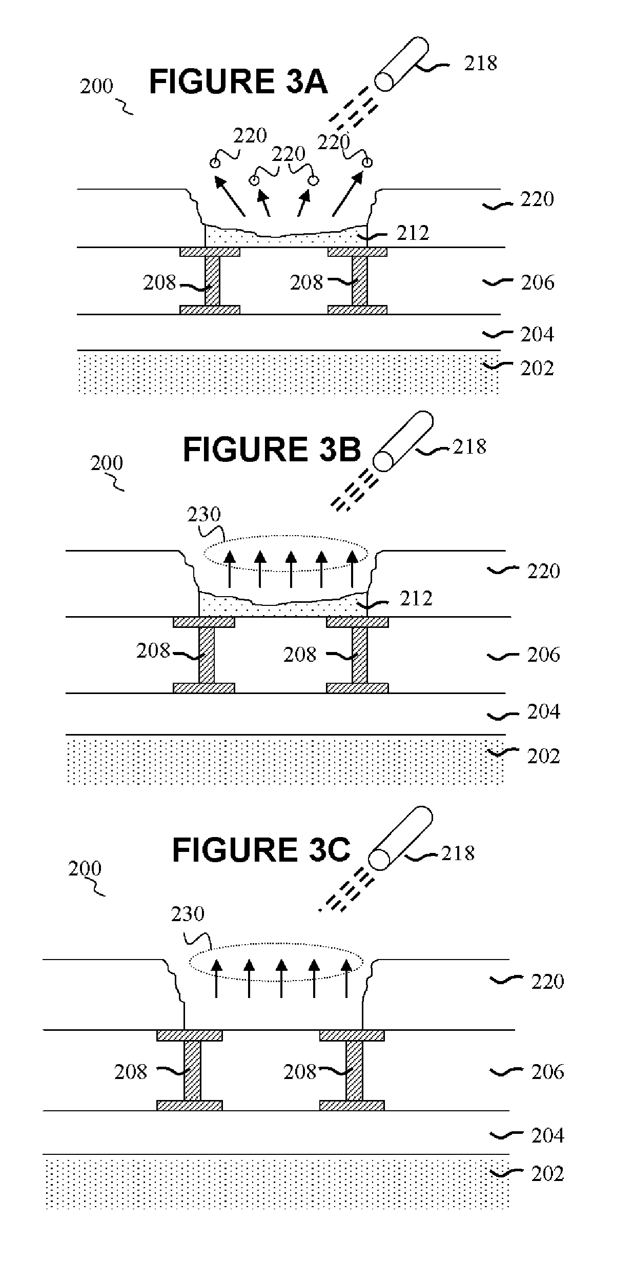
[0010] Initial reference is made to FIG. 1, which illustrates a conventional metal fuse within a semiconductor device 100. A plurality of integrated circuit (IC) interconnect layers 104 are formed on a semiconductor substrate102 utilizing known materials and methods. The semiconductor substrate 102 is preferably silicon, although silicon-on-insulator (SOI) and gallium arsenide (GaAs) substrates may also be utilized. The various interconnect layers 104 include but are not limited to interlevel metal dielectrics, gate electrodes, interlevel dielectrics, isolation regions, active and passive devices, capacitors and other features. The various interconnect layers 104 may also contain metal contacts (not shown) that electrically connected one layer to another.

[0011] An overlying intermetal dielectric (IMD) layer 106 is subsequently formed over the plurality of interconnects 104 using known materials and methods. The IMD layer 106 may include doped or undoped silicon oxide, fluorinated s...


PUM


Abstract

Described is a metal fuse in a semiconductor device that can be readily blown up without compromising device reliability, as well as methods of manufacturing thereof. In one embodiment, a metal fuse structure according to the disclosed principles comprises a semiconductor substrate, and an interconnect layers located on the semiconductor substrate, where the interconnect layer has metal contacts formed through the interconnect layer. In addition, the structure includes a metal fuse formed over the interconnect layer and in electrical contact with the metal contacts. Furthermore, the structure includes a polymeric coating formed over the metal fuse and the interconnect layer, where the polymeric coating is selected to allow radiation to pass therethrough.

Description

TECHNICAL FIELD [0001] This disclosure relates in general to semiconductor devices, and more particularly to a metal fuse structure for semiconductor devices and fabrication methods thereof. BACKGROUND [0002] Metal fuses are used in repairing semiconductor circuits and devices. Often times, the repair process involves breaking, severing, or vaporizing metal fuses with a laser beam. For example, there can be multiple memory and redundant cells within a memory device, and when defective memory cells are detected, metal fuses in redundant cells may be “blown” in order to repair the defective memory cells by isolating functional parts of the circuit(s). Metal fuses in redundant cells may also be opened or blown to re-route circuitry along alternative pathways in the event of a memory cell failure. In addition, it is also common to design and fabricate a generic logic chip having a large number of logic gate interconnects. Subsequently, the chip can be customized to perform the desired c...

Claims


Application Information

Patent Timeline
IPC IPC(8): H01L29/00
CPCH01L23/5258H01L2924/0002H01L2924/00
Inventor JENG, SHIN-PUU
Owner TAIWAN SEMICON MFG CO LTD
Why Eureka
Try Eureka