Thin film transistor array panel

a transistor array and thin film technology, applied in non-linear optics, instruments, optics, etc., can solve the problems of reducing the quality of the substrate, reducing the efficiency of the lcd manufacturing process, and easy damage of the tft channel near the pad, so as to minimize the defect of the pixel and reduce the manufacturing cos

Inactive Publication Date: 2007-03-22
SAMSUNG DISPLAY CO LTD
View PDF12 Cites 17 Cited by
  • Summary
  • Abstract
  • Description
  • Claims
  • Application Information

AI Technical Summary

Benefits of technology

[0017] It is another object of the present invention to provide a liquid crystal display which prevents electrostatic charges from entering into the substrate after a shorting bar is removed, thereby minimizing pixel defects.
[0018] It is yet another object of the present invention to provide a manufacturing method of a liquid crystal display in which an LCD panel is prevented from becoming damaged by an electrostatic discharge, while manufacturing costs of the LCD are reduced.
[0026] In the manufacturing method of the LCD, it is possible to protect the LCD panel against electrostatic charges generated during the manufacturing process since the step of cutting the substrate, of injecting liquid crystals and of sealing an injection hole are performed while the shorting bar remains on the LCD panel. Moreover, it is possible to reduce manufacturing costs since polarizers are attached on only the good LCD panels.

Problems solved by technology

This may cause the insulating films or TFTs to become damaged by the electrostatic discharge.
In the LCD manufacturing process, since the electrostatic charges, which is generated after the step of assembling the TFT substrate and a color filter substrate is completed, cause high voltages even though the amount of the charges are small, the quality of the substrate decreases.
In addition, since the electrostatic charge Is usually generated during the step of cutting the substrate, then flow into an active area having the pixel regions through gate and data pads, the channels of the TFTs near the pads become damaged by the electrostatic discharge with easy.
If electrostatic charges are generated in the pad area 30 and moves Inside the active area 40, the channels of the TFTs, which are located near the pads, become damaged, or the quality of the channels is deteriorated.
However, in the case where an amount of the electric charges is large, it is not possible to completely prevent damage caused by the electrostatic discharge.
Moreover, after the shorting bar is removed, it is not possible to prevent the electrostatic charges from entering into the substrate.
As mentioned above, since the shorting bar is removed in the same step of cutting the substrate, it is difficult to protect the substrate against the electrostatic charges after the step of removing the shorting bar.
In which only one signal is applied to every wire, by using the shorting bar, there is a high possibility that the polarizers are attached even on the damaged LCD panel.
If the damaged panel is detected in the post-test, the panel, along with the expensive polarizers, has to be discarded, thereby increasing overall manufacturing costs of the LCD.

Method used


Image

  • Thin film transistor array panel
  • Thin film transistor array panel
  • Thin film transistor array panel

Examples


second embodiment

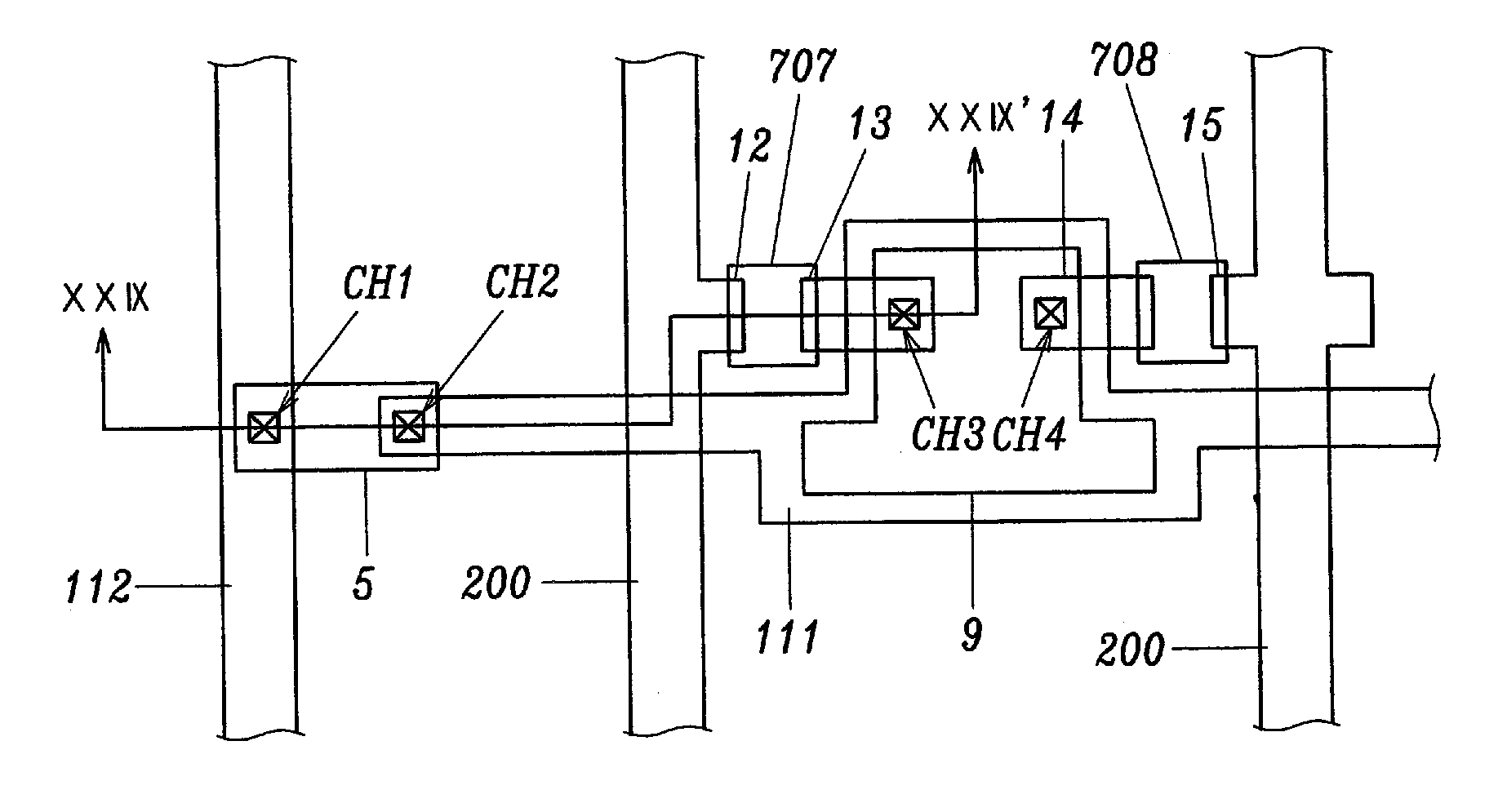
[0079]FIG. 6 is an enlarged view of the area A in FIG. 3 according to a second preferred embodiment of the present invention. In the second embodiment, electrostatic discharge protection circuits are located inside the area enclosed by the seal area 90.

[0080] As shown in FIG. 6, spark inducing circuits 130 are connected to wires 100 at the position between the seal area 90 and the active area line 41, and electrostatic discharge protection diode circuits 120 are connected to the wires 100 as in the previous embodiment. First and second electrostatic charging circuits (not shown) may be provided inside the area enclosed by the seal area 90.

[0081] A various types of the spark inducing circuits 130 according to the preferred embodiments are shown in FIGS. 7 to 11. First to fourth spark inducing circuits ST1, ST2, ST3 and ST4 will be described with reference to FIGS. 7 to 10, respectively, the first to fourth spark inducing circuits ST1, ST2, ST3 and ST4 representing the different type...

first embodiment

[0120] As described in the electrostatic charge discharging pattern of the first embodiment, the ends of the first to the fourth electrode pattern 118, 128, 119 and 129 are pointedly formed. The first and the third electrode patterns 118 and 119 respectively face the second and the fourth electrode patterns 128 and 129. The first and the second patterns 118 and 128 are formed on the first amorphous silicon pattern 704, and the third and fourth patterns 119 and 129 are formed on the second amorphous silicon pattern 705. Thus, the electrostatic charges flowing through the dummy data line 110 are discharged to the ITO pattern 302 for the capacitor through the pointed portion and stored in the capacitor. The number of the discharging devices D1 and D2 which are connected to the dummy data line 110 may be increased as required.

[0121]FIG. 24 shows a layout view of a electrostatic charge discharging pattern according to a third preferred embodiment of the prevent invention. As shown in FIG...

fourth embodiment

[0124] The electrostatic charge discharging pattern of the fourth embodiment can discharge electrostatic charges more effectively because one more capacitor is formed in the step of forming wires in the substrate.

[0125] Now, a manufacturing method of the electrostatic charge discharging patterns will be described hereinafter with references to FIGS. 21 to 25, and FIGS. 26A to 26F.

[0126] As shown in FIG. 26A, a metal layer for gate wires is deposited on a substrate 10 and patterned to form a gate line and a dummy gate line 100 respectively inside and outside. In the case of the electrostatic charge discharging pattern of the fourth preferred embodiment, a dummy metal line 130 is formed outside an active area in parallel with the gate and the dummy gate line 100 in this step.

[0127] As shown In FIG. 26B, a gate Insulating film 3 is deposited with silicon nitride or silicon oxide. Next, an amorphous silicon and a doped amorphous silicon are deposited and then patterned to form an amor...


PUM

PropertyMeasurementUnit
conductivityaaaaaaaaaa
insulatingaaaaaaaaaa
semiconductoraaaaaaaaaa

Abstract

A data line and an amorphous silicon pattern are formed on a substrate. The first electrode pattern is extended from the data line and overlaps an edge of the amorphous silicon pattern. The second electrode pattern is made of the same metal as the first electrode pattern and overlaps the edge of the amorphous silicon pattern at an opposite side of the first electrode pattern. Edges of the first and the second electrode patterns are sharply formed so that a tunneling effect easily occurs through the amorphous silicon pattern. An indium-tin-oxide pattern for a capacitor is formed at the end of the second electrode pattern. The capacitor is formed between the ITO pattern and a common electrode.

Description

RELATED APPLICATIONS [0001] This application is a continuation application of U.S. patent application Ser. No. 10 / 465,883, filed Jun. 20, 2003, which is herein incorporated by references for all purposes.BACKGROUND OF THE INVENTION [0002] (a) Field of the Invention [0003] The present invention relates to liquid crystal displays (referred to as an LCD hereinafter) and manufacturing methods thereof, and more particularly, to circuits for preventing electrostatic discharge which are provided in the LCD and manufacturing methods thereof. [0004] (b) Description of the Related Art [0005] A liquid crystal display (LCD), which is one type of flat panel display (FPD), includes two substrates having transparent electrodes and a liquid crystal layer interposed between the substrates. In the LCD, light transmittance is controlled by varying the voltages applied to the liquid crystal layer. [0006] On a thin film transistor (TFT) substrate of the LCD, N gate lines and M data lines, which cross ea...

Claims


Application Information

Patent Timeline
Patent Type & Authority Applications(United States)
IPC IPC(8): G02F1/1333G02F1/1362G02F1/365
CPCG02F2001/133388G02F1/136204G02F1/133388
Inventor LEE, JOO-HYUNGKIM, DONG-GYUPARK, WOON-YONG
Owner SAMSUNG DISPLAY CO LTD
Why Eureka
Try Eureka