Mobility enhancement by strained channel CMOSFET with single workfunction metal-gate and fabrication method thereof

a technology of strained channel and metal gate, which is applied in the direction of semiconductor devices, semiconductor/solid-state device details, electrical apparatus, etc., can solve the problems of poly-si having problems of poly depletion and sheet resistance, significant increase in leakage current, and inability to control the current, etc., to achieve the effect of improving hole mobility and enhancing electron mobility

Inactive Publication Date: 2007-03-29
IND TECH RES INST
View PDF5 Cites 14 Cited by
  • Summary
  • Abstract
  • Description
  • Claims
  • Application Information

AI Technical Summary

Benefits of technology

[0012] According to the invention, a method and a device for mobility enhancement by strained channel CMOSFET with single workfunction metal-gate are provide

Problems solved by technology

As a result, the leakage current is significantly increased with a direct tunneling effect, and the controllability issue still exists.
When IC dimensions decrease, the poly-Si has issues of poly depletion and sheet resistance.
The former, however, is a complex process, and the latter is limited by solid solubility.
However, the tensile strained Si cannot significantly improve the hole mobility in PMOSFET.
This method requires a SiGe virtual substrate that lea

Method used


Image

  • Mobility enhancement by strained channel CMOSFET with single workfunction metal-gate and fabrication method thereof
  • Mobility enhancement by strained channel CMOSFET with single workfunction metal-gate and fabrication method thereof
  • Mobility enhancement by strained channel CMOSFET with single workfunction metal-gate and fabrication method thereof

Examples


Embodiment Construction

[0021] The following description is of the best-contemplated mode of carrying out the invention. This description is made for the purpose of illustrating the general principles of the invention and should not be taken in a limiting sense. The scope of the invention is best determined by reference to the appended claims.

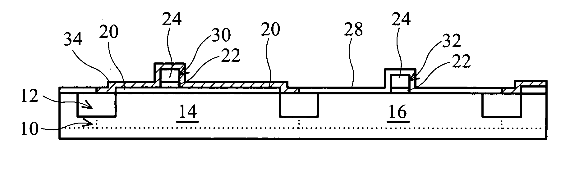
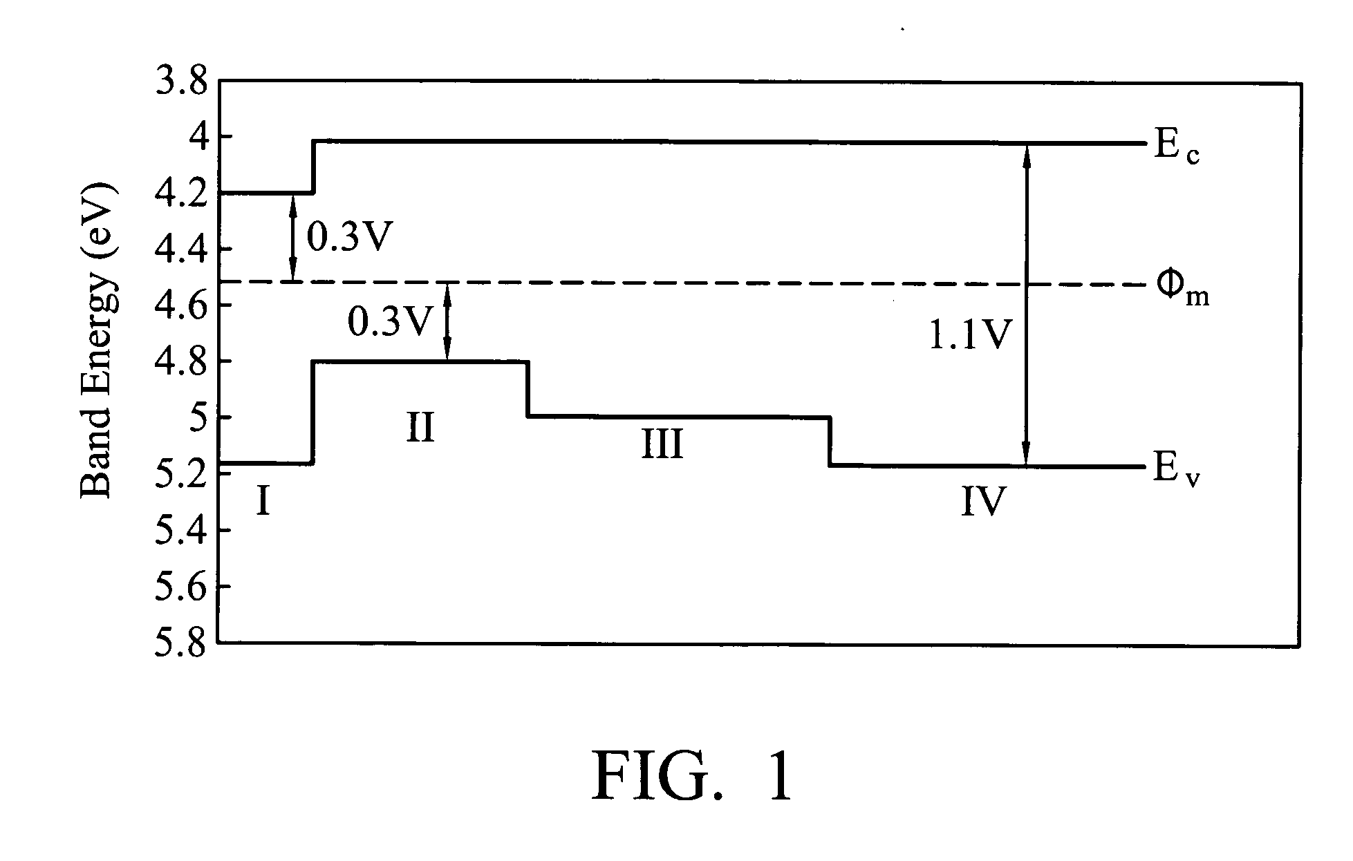
[0022] A mobility enhancement by strained channel CMOSFET with single workfunction metal gate will be described here in greater detail. Some embodiments of the invention, such as the exemplary embodiments described can potentially improve the hole and electron mobility of the PMOSFET and the NMOSFET, respectively. The single workfunction metal gate is further combined with high-k materials. In some embodiments, this can be accomplished by forming a compressively strained SiGe channel in the PMOSFET region, and a tensile cap layer in the NMOSFET region to produce a local tensile stress on the NMOSFET channel.

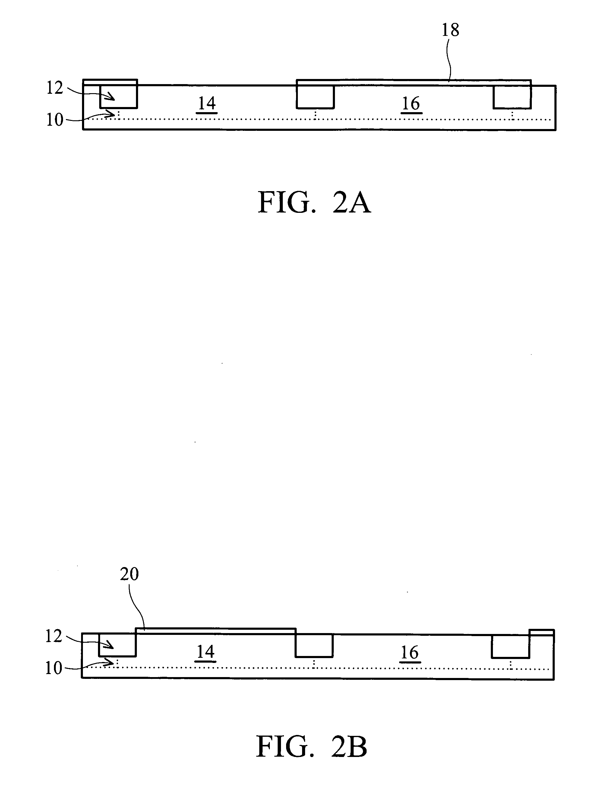
[0023] Referring now to the drawings, FIG. 2A is a schemati...


PUM


Abstract

The present invention provides a complementary metal-oxide-semiconductor (CMOS) device and a fabrication method thereof. The CMOSFET device includes a compressively strained SiGe channel for a PMOSFET, as well as a tensile strained Si channel for an NMOSFET, thereby enhancing hole and electron mobility for the PMOSFET and the NMOSFET, respectively. As such, the threshold voltages of the two types of transistors can be obtained in oppositely symmetric by single metal gate.

Description

BACKGROUND OF THE INVENTION [0001] 1. Field of the Invention [0002] The present invention relates to complementary metal-oxide-semiconductor (CMOS) technology. More particularly, it relates to combining a compressively strained SiGe channel of a PMOSFET with a local tensile strained Si channel of an NMOSFET, such that a band gap narrowing of the CMOSFET and improving holes and electrons mobility of the PMOSFET and NMOSFET, respectively. [0003] 2. Description of the Related Art [0004] The density of integrated circuits (IC) continues to increase and feature size thereof continues to scale down, improving the performance of IC devices and lowering manufacturing costs. Shorter channel length causes gate electrodes to lose channel controllability due to the short channel effect (SCE). This controllability problem can be solved by reducing the thickness of the gate dielectric layer (silicon dioxide), and this decreases the operating voltage and increases driving current. As a result, the...

Claims


Application Information

Patent Timeline
IPC IPC(8): H01L23/62
CPCH01L21/265H01L21/823807H01L21/823864H01L29/1054H01L29/4966H01L29/517H01L2924/0002H01L29/78H01L29/7843H01L2924/00
Inventor LU, SHIN-CHIILIN, YU-MINGLEE, MIN-HUNGPEI, ZING-WAYHSIEH, WEN YI
Owner IND TECH RES INST
Why Eureka
Try Eureka