Junction barrier schottky (JBS) with floating islands

a junction barrier and floating island technology, applied in the field of junction barrier schottky (jbs) with floating islands, can solve the problems of low schottky barrier height, difficulty in applying junction barrier schottky (jbs), and other problems, to achieve the effect of improving jbs performance, reducing forward voltage, and increasing breakdown voltag

Active Publication Date: 2007-04-05
ALPHA & OMEGA SEMICON LTD
View PDF13 Cites 43 Cited by
  • Summary
  • Abstract
  • Description
  • Claims
  • Application Information

AI Technical Summary

Benefits of technology

[0009] It is therefore an aspect of the present invention to provide a new and improved Schottky diode with the junction barrier metal deposited in the trenches with dopant region disposed below the trenches that has a grading dopant profiles by carrying out a tapered dopant implant for improving the JBS performance such that the above discussed limitations and difficulties of the convention Schottky is resolved.

Problems solved by technology

The trench Schottky diode configuration leads to another technical difficulty due to the performance limitations including the required high forward voltage VF, the low sustainable breakdown voltage BV, and the high leakage current Idss.
These performance limitations often cause difficulties in applying the junction barrier Schottky (JBS) for broader and more variety of applications.
Low Schottky barrier height will give rise to higher leakage current in the reverse blocking operation of the diode.
The disadvantage of the JBS is the reduced Schottky surface area from the p-type junctions.
The rounding of the sharp corners requires extra process steps and specialized equipment and all these requirements cause an increase in the production costs.

Method used


Image

  • Junction barrier schottky (JBS) with floating islands
  • Junction barrier schottky (JBS) with floating islands
  • Junction barrier schottky (JBS) with floating islands

Examples


Embodiment Construction

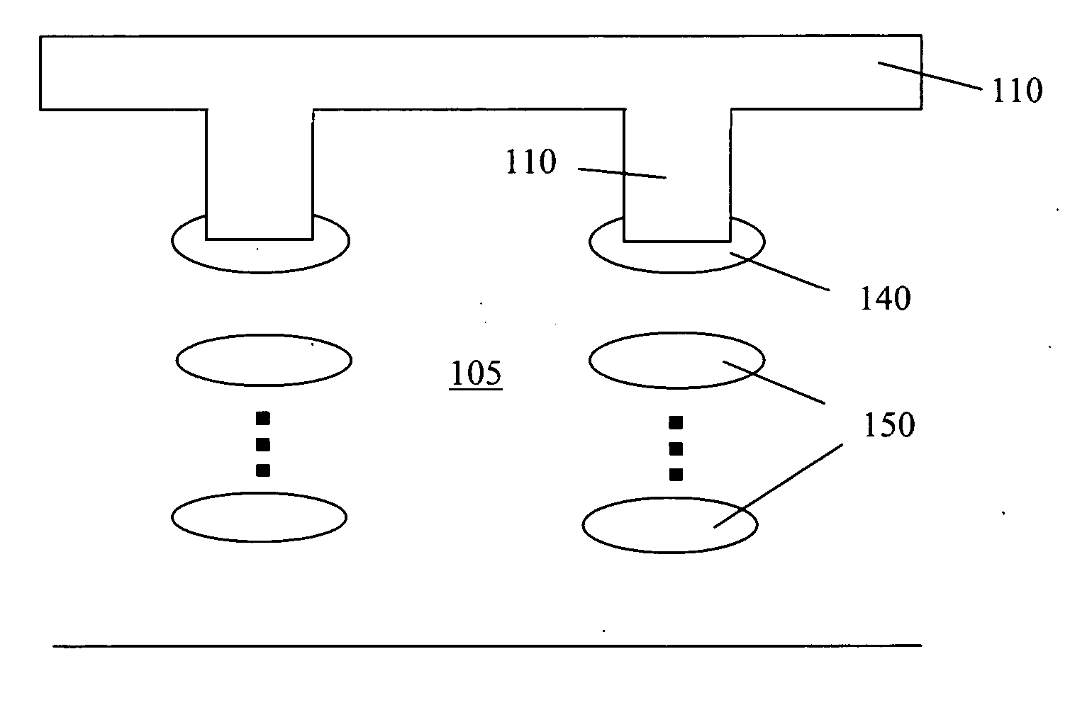
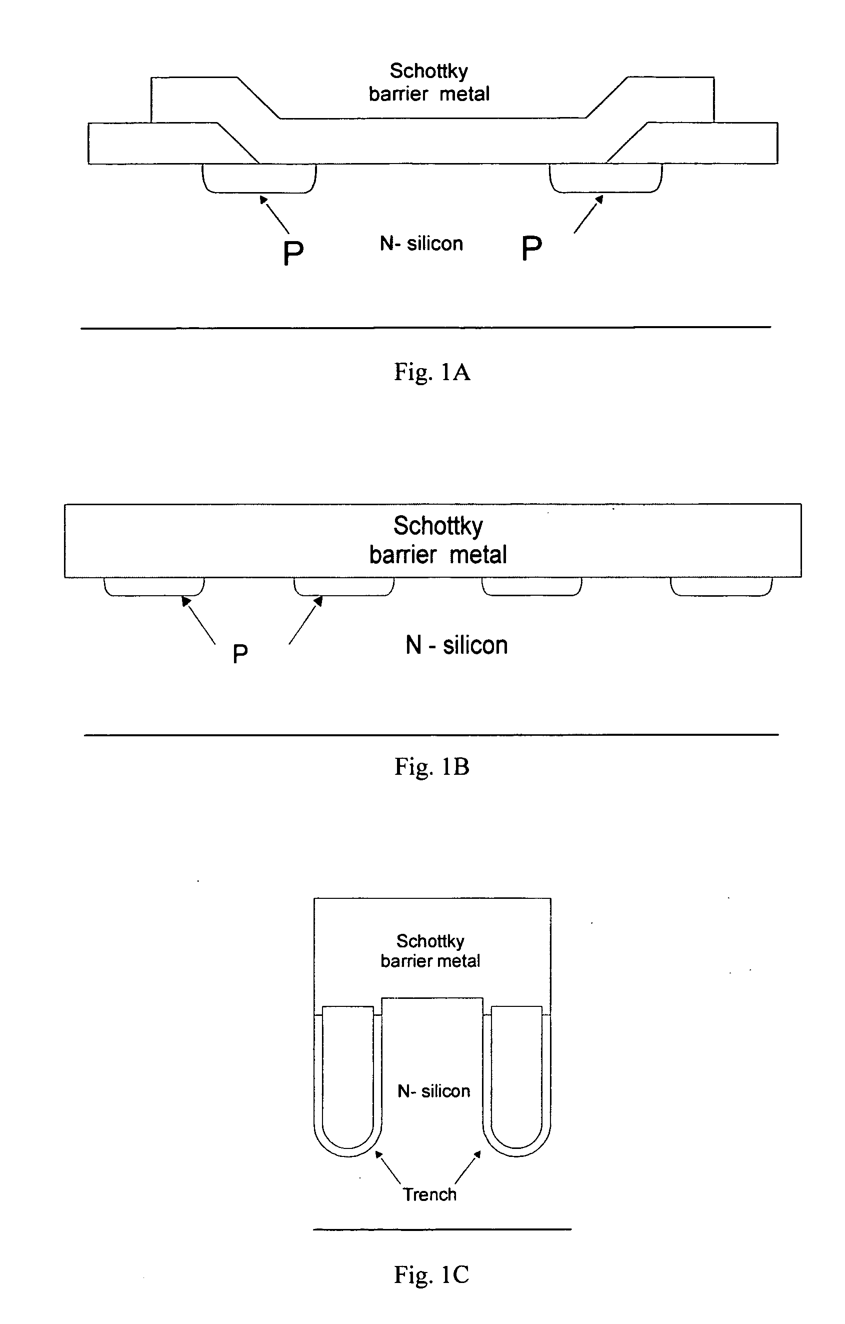
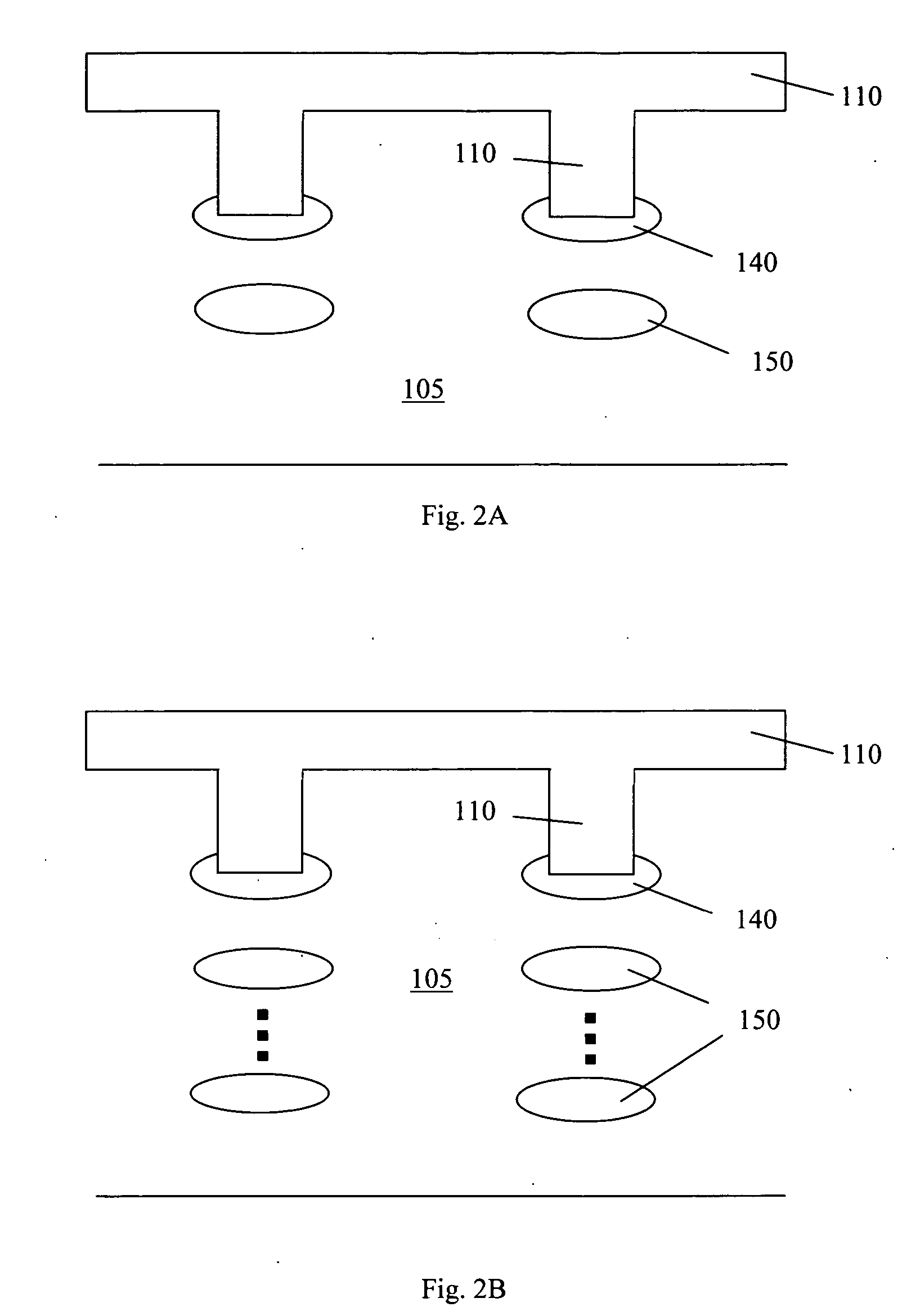
[0019] Referring to FIG. 2A for a cross sectional view of an Schottky diode 100 of this invention. The Schottky diode 100 is supported and formed in a semiconductor substrate, e.g., a N-doped silicon substrate 105. The Schottky diode 100 includes a plurality of trenches forming a plurality of semiconductor mesas. In the preferred embodiment as shown in FIG. 2 the trenches are filled with Schottky barrier metal, e.g., Ti / TiN or Tungsten metal 110, or a contact metal overlaying a Schottky barrier metal. In another preferred embodiment (not shown), at least a portion of vertical surface of semiconductor mesas is lined with Schottky barrier metal. For the purpose of preventing leakage current generated by the reverse voltage, P-dopant regions 140 are formed surrounding the bottom of the trenches. A floating P− island 150 is disposed underneath the trench bottoms. In reverse bias, the floating P island 150 forms an extra PN junction with substrate in addition to the PN junction formed be...


PUM


Abstract

A Schottky diode includes a Schottky barrier and a plurality of dopant regions disposed near the Schottky barrier as floating islands to function as PN junctions for preventing a leakage current generated from a reverse voltage. At least a trench opened in a semiconductor substrate with a Schottky barrier material disposed therein constitutes the Schottky barrier. The Schottky barrier material may also be disposed on sidewalls of the trench for constituting the Schottky barrier. The trench may be filled with the Schottky barrier material composed of Ti / TiN or a tungsten metal disposed therein for constituting the Schottky barrier. The trench is opened in a N-type semiconductor substrate and the dopant regions includes P-doped regions disposed under the trench constitute the floating islands. The P-doped floating islands may be formed as vertical arrays under the bottom of the trench.

Description

[0001] This Patent Application is a Continuation in Part (CIP) Application of a co-pending Application with a Ser. No. 11 / 056,345 filed by a common Inventor of this Application on Feb. 11, 2005. The Disclosures made in that Application is hereby incorporated by reference.BACKGROUND OF THE INVENTION [0002] 1. Field of the Invention [0003] The invention relates generally to the semiconductor power devices. More particularly, this invention relates to an improved and novel manufacturing process and device configuration for providing the MOSFET device with shielded trench gates with cells provided with Schottky source contact for improving performance of high frequency power switching, H-bridge and synchronization rectification applications. [0004] 2. Description of the Related Art [0005] As the applications of Schottky diodes become more widespread, particularly for reducing the power consumption and increasing the switching speed, it becomes even more important to improve the device c...

Claims


Application Information

Patent Timeline
Patent Type & Authority Applications(United States)
IPC IPC(8): H01L29/47
CPCH01L29/0623H01L29/1095H01L29/407H01L29/66727H01L29/66734H01L29/7811H01L29/782
Inventor PAN, JIBHALLA, ANUP
Owner ALPHA & OMEGA SEMICON LTD
Why Eureka
Try Eureka