Semiconductor device manufacturing system

Inactive Publication Date: 2007-04-05
TOKYO ELECTRON LTD
View PDF5 Cites 10 Cited by
  • Summary
  • Abstract
  • Description
  • Claims
  • Application Information

AI Technical Summary

Benefits of technology

[0015] In a typical embodiment, the particle detecting part is configured to output data, as the detection result, in which representative values each representing a state of particle adhesion in each minute areas (a square-shaped area 0.1 mm to 0.5 mm on a side, for example) defined by dividing a surface of the substrate are correlated with addresses of the respective minute areas. In the evaluation data, evaluation values, each representing the state of particle adhesion in each of evaluation areas defined by dividing a surface of the substrate, are correlated with addresses of the respective evaluation areas. The eval

Problems solved by technology

When a malfunction, resulting in an undesirable treatment result (i.e., adhesion of particles), occurs in one semiconductor device manufacturing apparatus, the succeeding treatment steps become useless.
In the computer used with the semiconductor device manufacturing apparatus, the performance of the processor is poor and a memory capacity is small.
Thus, it is practically very difficult for the computer used with the semiconductor device manufacturing apparatus to execute a calculation for estimating the cause of particle generation by using such vast amounts of inspection data as they are.
It is also very difficult to transfer such vast amounts

Method used


Image

  • Semiconductor device manufacturing system
  • Semiconductor device manufacturing system
  • Semiconductor device manufacturing system

Examples


Embodiment Construction

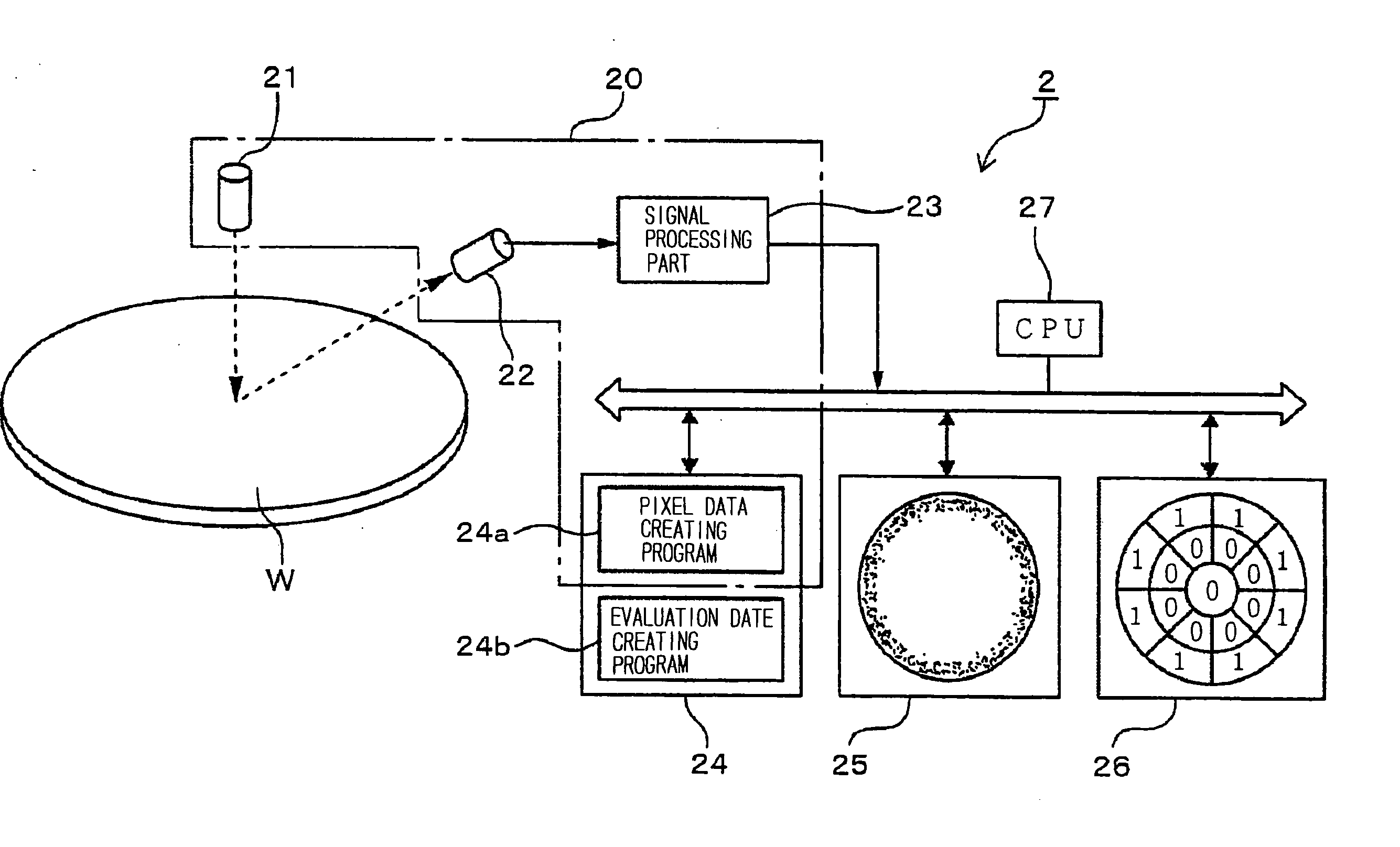
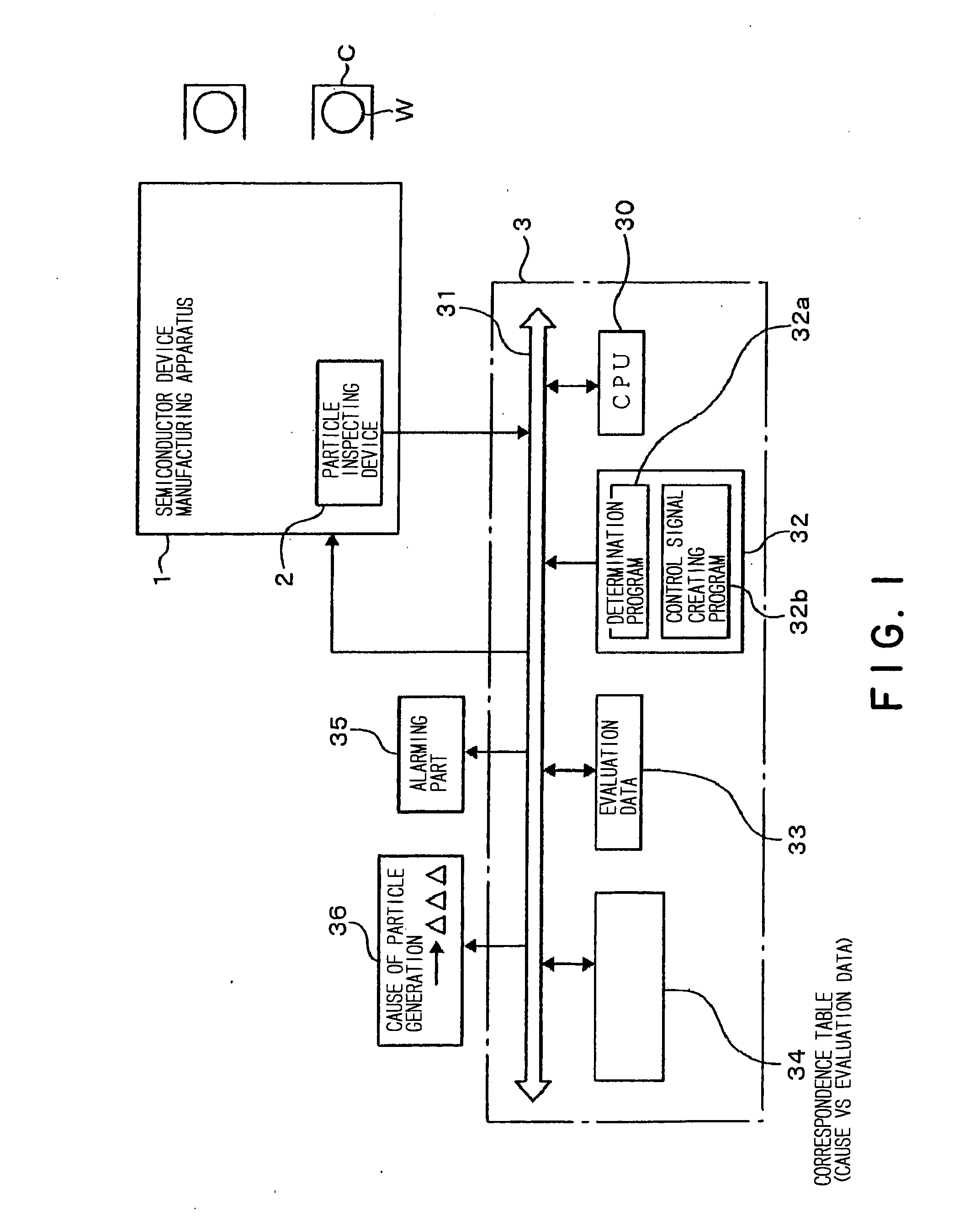
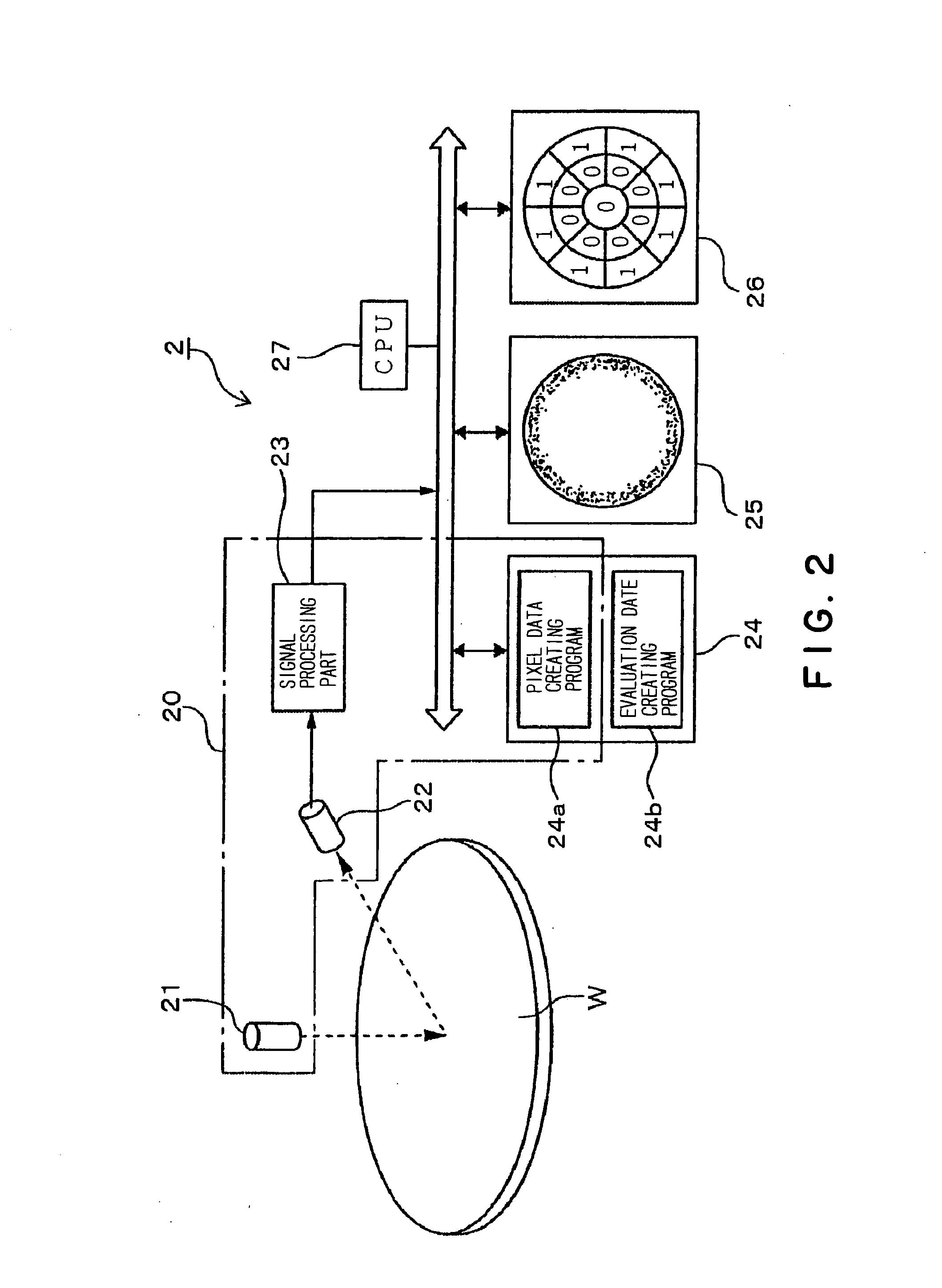
[0038]FIG. 1 is shows the structure of a semiconductor device manufacturing system in one embodiment of the present invention. The semiconductor device manufacturing system includes a semiconductor device manufacturing apparatus 1. The semiconductor device manufacturing apparatus 1 is a substrate processing apparatus that performs a treatment for forming a semiconductor integrated circuit on a substrate such as a semiconductor wafer or a glass substrate for a liquid crystal display. The semiconductor device manufacturing apparatus 1 may be a heat treatment apparatus, an etching apparatus, a film-deposition apparatus, a spattering apparatus, an ion implantation apparatus, an ashing apparatus, a coating and developing apparatus that applies a resist liquid on a substrate and develops the substrate after it is exposed, a cleaning apparatus, and so on. Not limited to the above apparatuses that directly treats a substrate, the semiconductor device manufacturing apparatus 1 may be other a...


PUM


Abstract

The present invention provides a system capable of automatically making a diagnosis of a semiconductor device manufacturing apparatus, based on a result of particle detection on a substrate such as a semiconductor wafer. In one preferred embodiment, the surface of the wafer is divided into square-shaped minute areas of 0.1 mm to 0.5 mm, and existence of particles in each minute area is inspected. Based on the inspection result, data, in which existence of particles in each minute area is correlated with the address thereof, is created. The surface of the wafer is divided into several tens to several hundreds of evaluation areas. A binarized data is assigned to each evaluation area, and is determined based on the fact that the number of the minute areas in which particles are detected included in the evaluation area is larger, or not larger than a predetermined reference value. A correspondence table, showing the relationship between binarized data arrangements and the causes of particle adhesion, which is made based on empirical rules or experimental results, is prepared. By applying the binarized data made based on the inspection result to the correspondence table, the cause of particle adhesion can be identified.

Description

TECHNICAL FIELD [0001] The present invention relates to a semiconductor device manufacturing system having functions of detecting particles adhered to a substrate, such as a semiconductor wafer, which has been subjected to a predetermined treatment by a semiconductor device manufacturing apparatus, and of determining the cause of particle adhesion based on the detection result. BACKGROUND ART [0002] Semiconductor device manufacturing apparatuses used in a series of treatment steps for manufacturing a semiconductor integrated circuit includes, for example, a film-deposition apparatus, an etching apparatus, a coating and developing apparatus for applying a resist to a wafer and developing the same, and a cleaning apparatus for cleaning a wafer. When a malfunction, resulting in an undesirable treatment result (i.e., adhesion of particles), occurs in one semiconductor device manufacturing apparatus, the succeeding treatment steps become useless. Thus, conditions of the respective appara...

Claims


Application Information

Patent Timeline
IPC IPC(8): G06K9/00G01N21/956G01N21/95H01L21/66
CPCG01N21/94G01N21/9501H01L22/00
Inventor YATSUGAKE, YASUOKATO, HITOSHIYASUHARA, MOYURUIRIE, TAKASHI
Owner TOKYO ELECTRON LTD
Why Eureka
Try Eureka