
System and method for making an improved thin film solar cell interconnect

a solar cell and interconnection technology, applied in the field of photovoltaic devices, can solve the problems of increasing optical transmission loss through, reducing the efficiency of modules, so as to improve module quality and yield, simplify the overall process, and simplify the effect of the process

Inactive Publication Date: 2007-04-12
APPLIED MATERIALS INC
View PDF32 Cites 107 Cited by
  • Summary
  • Abstract
  • Description
  • Claims
  • Application Information

AI Technical Summary

Benefits of technology

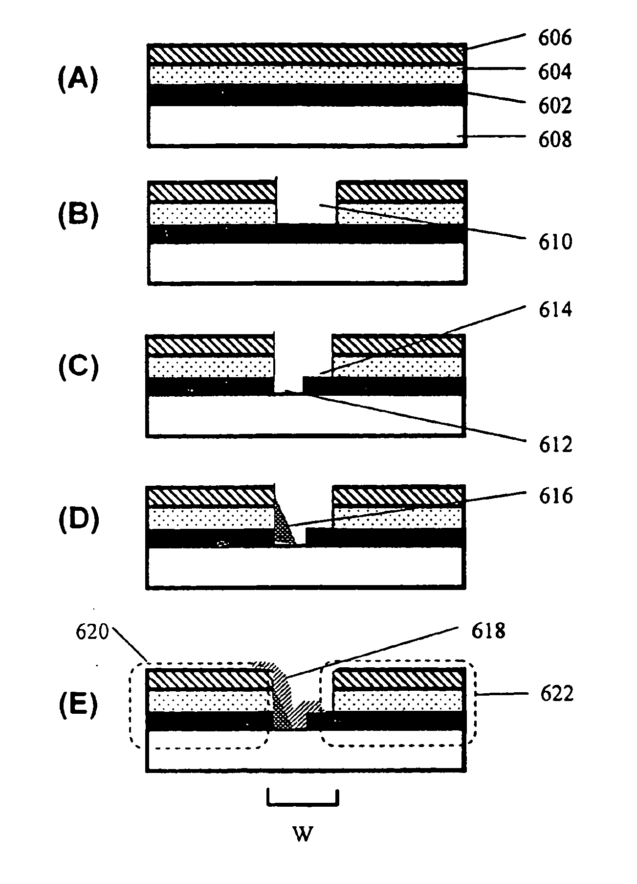
[0015] According to one aspect, a method according to the invention includes forming the module interconnect with a single cutting process after the deposition of all active layers. This simplifies the overall process to a set of vacuum steps followed by a set of interconnect steps, and may significantly improve module quality and yield.
[0016] According to another aspect, a method according to the invention includes self-aligned deposition of an insulator. This simplifies the process because no alignment is required, and reduces the area used for interconnect, because no width is required to take up alignment errors.
[0017] According to another aspect, a method according to the invention includes a scribing process that results in a much narrower interconnect which may significantly boost module efficiency, and allow for narrower cell sizes.
[0018] According to another aspect, an interconnect according to the invention includes an insulator layer that greatly reduces shunt current through the active layer, which can greatly improve module efficiency.

Problems solved by technology

This increases optical transmission loss through the TCO, causing a loss of about 10% of the module efficiency.
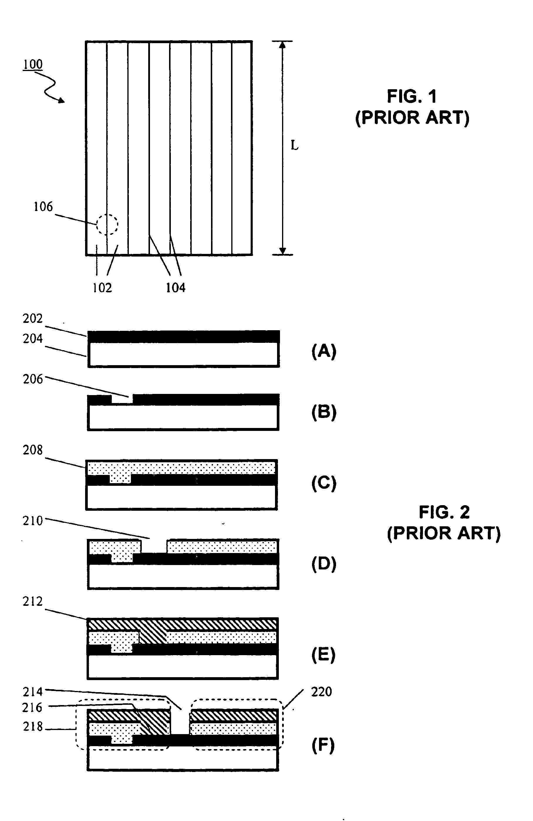
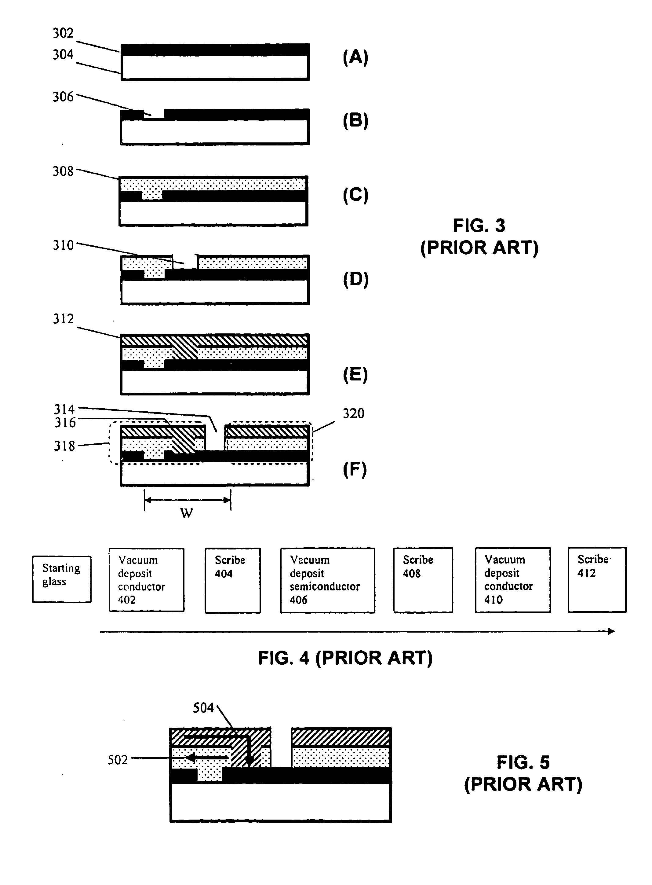
However, such attempts have been unsatisfactory because, for example, (1) they rely on multiple scribes that must be aligned to one another (which is difficult due to registration errors in the scribes over a long distance) and (2) they do not suppress the parasitic resistance, as will be described below.
Another problem with the module interconnects is that they contain a parasitic reverse resistor through the active layer of the semiconductor that can significantly degrade cell performance.
This can cause damage near the edge of the scribe, further decreasing efficiency of the resulting module.
Moreover, the multiple transitions between vacuum and air cause further contamination in the resulting module, and increase expense of the overall process because of the need for multiple load locks.
Still further, the air exposure in the middle of the deposition of active layers can degrade performance of the resulting module.
However, such techniques involving IC fabrication and lithography with masks are not practical for thin-film modules which are typically much greater than 10 cm on a side.
Moreover, such techniques are not readily extendable to thin-film solar cells because GaAs solar cells have no metal contact layers (e.g. layers corresponding to 202 and 212 in FIG. 2 or 302 and 312 in FIG. 3).

Method used


Image

  • System and method for making an improved thin film solar cell interconnect
  • System and method for making an improved thin film solar cell interconnect
  • System and method for making an improved thin film solar cell interconnect

Examples


Embodiment Construction

[0104] The present invention will now be described in detail with reference to the drawings, which are provided as illustrative examples of the invention so as to enable those skilled in the art to practice the invention. Notably, the figures and examples below are not meant to limit the scope of the present invention to a single embodiment, but other embodiments are possible by way of interchange of some or all of the described or illustrated elements. Moreover, where certain elements of the present invention can be partially or fully implemented using known components, only those portions of such known components that are necessary for an understanding of the present invention will be described, and detailed descriptions of other portions of such known components will be omitted so as not to obscure the invention. In the present specification, an embodiment showing a singular component should not be considered limiting; rather, the invention is intended to encompass other embodime...


PUM


Abstract

In a module of photovoltaic cells, a method of forming the module interconnects includes a single cutting process after the deposition of all active layers. This simplifies the overall process to a set of vacuum steps followed by a set of interconnect steps, and may significantly module quality and yield. According to another aspect, an interconnect forming method includes self-aligned deposition of an insulator. This simplifies the process because no alignment is required. According to another aspect, an interconnect forming method includes a scribing process that results in a much narrower interconnect which may significantly boost cell efficiency, and allow for narrower cell sizes. According to another aspect, an interconnect includes an insulator layer that greatly reduces shunt current through the active layer, which can greatly improve cell efficiency.

Description

FIELD OF THE INVENTION [0001] The present invention relates generally to photovoltaic devices, and more particularly to a system and method for making improved interconnects in thin-film photovoltaic devices. BACKGROUND OF THE INVENTION [0002] Thin film solar modules offer an attractive way to achieve low manufacturing cost with reasonable efficiency. These modules are made from a variety of materials, including amorphous silicon, amorphous silicon germanium, copper indium gallium selenide (CIGS), and cadmium telluride. A common feature of these solar modules is the deposition on a large area insulator such as a glass sheet. [0003] Another common feature of these modules is the use of scribes and interconnects to divide the large area deposited layer into a number of cells and / or sub-cells. A top view of a typical module divided in this fashion is shown in FIG. 1. As shown in FIG. 1, a module 100 is divided into a plurality of cells 102 (i.e. stripes) that are series connected (e.g....

Claims


Application Information

Patent Timeline
IPC IPC(8): H02N6/00H01L31/00
CPCH01L31/046Y02E10/50H01L31/0465H01L31/0463
Inventor BORDEN, PETER G.EAGLESHAM, DAVID J.
Owner APPLIED MATERIALS INC
Learn More