Eureka AIR delivers breakthrough ideas for toughest innovation challenges, trusted by R&D personnel around the world.

Plasma display panel

Inactive Publication Date: 2007-04-12
PANASONIC CORP
View PDF4 Cites 11 Cited by
  • Summary
  • Abstract
  • Description
  • Claims
  • Application Information

AI Technical Summary

Benefits of technology

[0017] According to a PDP of the present invention, the amount of secondary electron emission produced when high energy ions and electrons collide with the protective film increases through the action of the needle crystals disposed to penetrate the dielectric film or the protective film in a thickness direction. Consequently, power consumption can be greatly reduced because of the increased luminous efficiency, as well as contributing to the reduction in discharge firing voltage and the suppression of discharge variability in the PDP.
[0018] Here, an excellent reduction in the discharge firing voltage is achieved, because electrons are efficiently emitted by disposing the needle crystals substantially perpendicular to the main surface of the front substrate, and layering the materials of the protective film and the dielectric film to completely fill the gaps between the needle crystals, and also by forming a phase-separated structure with the dielectric film and the needle crystals.
[0019] Electrons are supplied from the electrodes to the discharge space via the needle crystals following the application of a voltage to the electrodes, particularly in the case where the needle crystals are disposed substantially perpendicular to the main surface of the front substrate to penetrate the dielectric film in a thickness direction, and the dielectric film material and the protective film material are layered to completely fill the gaps between the needle crystals. In this way, the discharge firing voltage and discharge variability can be reduced, even through the action of electrons supplied to the discharge space via the needle crystals when a voltage is applied to the electrodes.
[0020] Here, electrons are supplied directly to the discharge space in the case where the tips of the needle crystals are exposed in the discharge space. However, even if the tips of the needle crystals are buried in the protective film rather than being exposed in the discharge space, cracks normally form in the protective film between crystals constituting the protective film, thus allowing for electrons to be supplied from the tips of the needle crystals to the discharge space through these cracks. Also, burying the tips of the needle crystals in the protective film improves durability.
[0021] On the other hand, with the PDP of the present invention, the protective film remains insulated from the electrodes in areas of the dielectric film other than those penetrated by the needle crystals, thereby enabling the wall-charge holding performance of the protective film surface over these areas to be ensured.
[0022] Furthermore, since the surface area of the protective film does not need to be enlarged by creating surface unevenness, the protective film need not be thinly formed. Consequently, patchiness in the formation of the protective film can be eliminated, and variability in secondary electron emission performance can also be suppressed.

Problems solved by technology

Reducing power consumption and suppressing discharge variability remain ongoing problems to be resolved in PDPs having the above features, with attempts having been made to resolve these problems from the angle of panel structure, drive method, and materials.

Method used


Image

  • Plasma display panel
  • Plasma display panel
  • Plasma display panel

Examples


embodiment 1

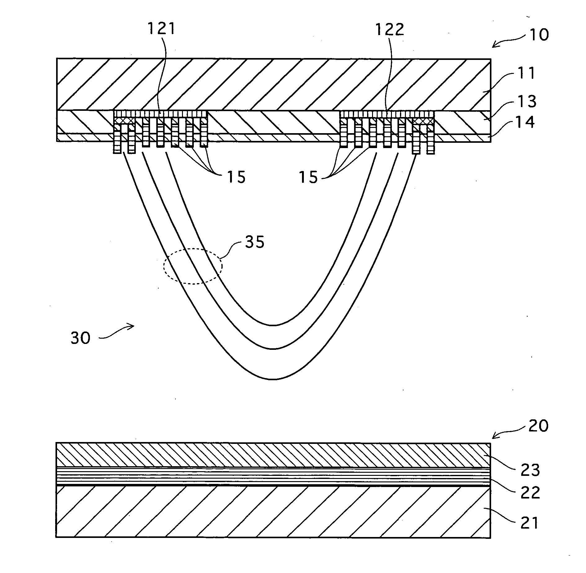
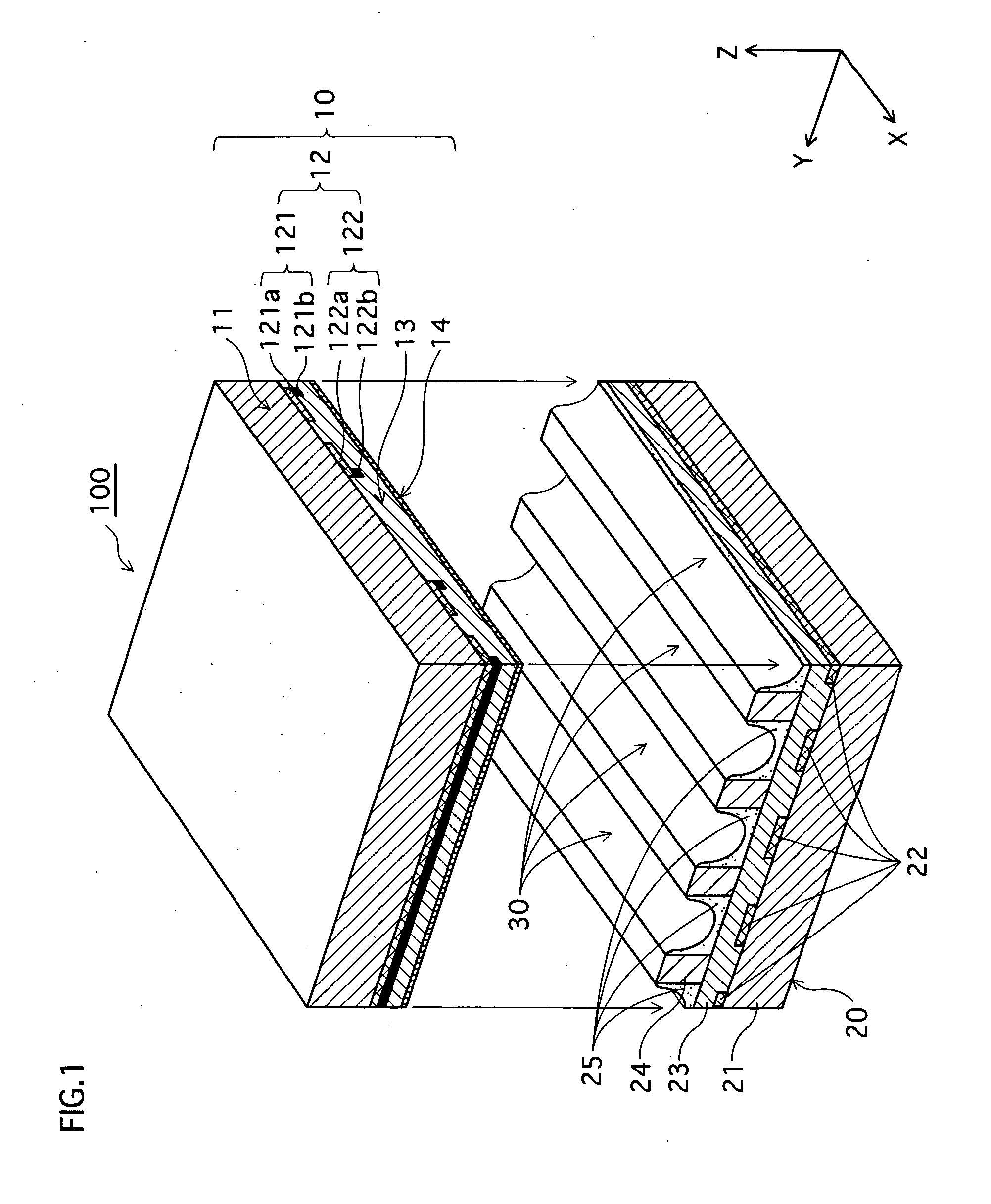
[0069]FIG. 1 is a perspective view showing a main section of the configuration of a PDP pertaining to preferred embodiments of the present invention.

[0070] PDP 100 is constituted from a front panel and a back panel that are stuck together.

[0071] Front panel 10 is constituted from a plurality of display electrode pairs 12 (scan electrodes 121 and sustain electrodes 122) formed in stripes on one side of a front substrate 11 composed of glass plate, and a first dielectric film 13 and a protective film 14 layered to cover the electrodes.

[0072] On the other hand, back panel 20 is constituted from a plurality of data electrodes 22 formed in stripes on one side of a back substrate 21 composed of glass plate, a second dielectric film 23 layered to cover data electrodes 22, barrier ribs 24 formed on second dielectric film 23 between data electrodes 22, and phosphor film 25 applied to the surface of second dielectric film 23 and to the side walls of barrier ribs 24.

[0073] Front substrate ...

embodiment 2

[0122] The overall PDP configuration is similar to embodiment 1.

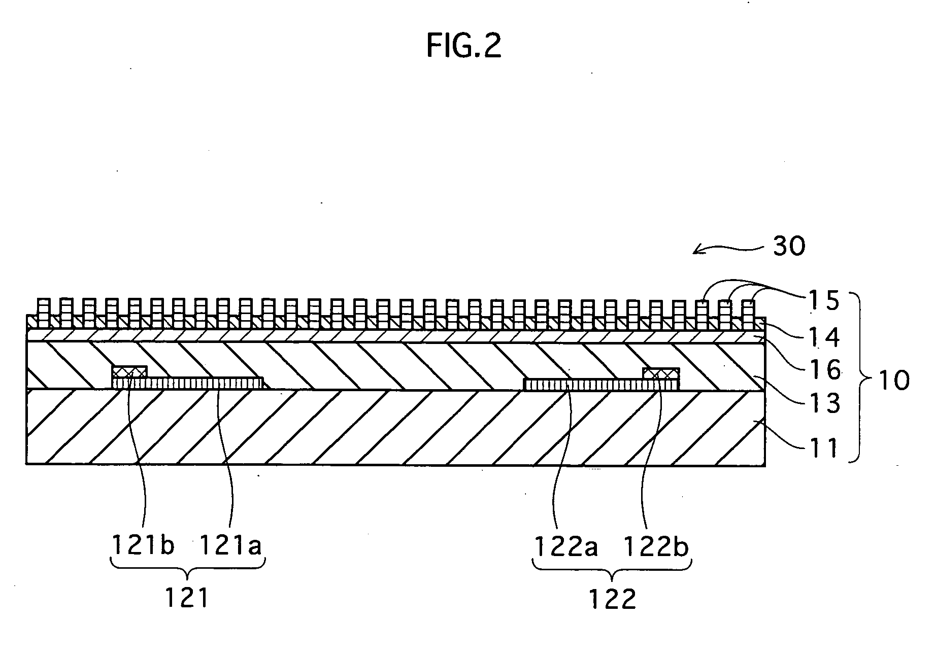
[0123]FIG. 6 is a perspective view of a main section of front panel 10 in embodiment 2.

[0124] This front panel 10 is constituted from a plurality of display electrode pairs 12 formed in stripes on one side of a front substrate 11 composed of glass plate, and a first dielectric film 13 and a protective film 14 layered to cover these electrode pairs. Tetrapod-shaped needle crystal particles 40 are disposed on the surface of first dielectric film 13, and penetrate protective film 14. Needle crystal particles 40 are formed using a conductive substance or a semiconductor substance.

[0125] Needle crystal particles 40 disposed on the surface of first dielectric film 13 each have four arms owing to their tetrapod shape. Three of these arms contact the surface of first dielectric film 13, while the fourth arm stands perpendicular to the surface of first dielectric film 13. Consequently, the needle crystals stand upright on the...

embodiment 3

[0137] The overall PDP configuration is similar to embodiment 1.

[0138]FIGS. 7 and 8 show configurations of front panel 10 pertaining to the present embodiment.

[0139]FIGS. 7A and 8A are schematic cross-sectional views of front panel 10, while FIGS. 7B and 7C are schematic plan views of front panel 10. FIG. 8B is a partially enlarged view of FIG. 8A.

[0140] Needle crystals 15 are disposed in an upright position on the surface of display electrodes 121 and 122, and penetrate first dielectric film 13, as shown in FIGS. 7A and 8A. Needle crystals 15 are formed using a conductive substance or a semiconductor substance. With front panel 10 shown in FIGS. 7A to 7C, the tips of needle crystals 15 are exposed in the discharge space above the surface of protective film 14, whereas in FIGS. 8A to 8B the tips of needle crystals 15 remain within protective film 14 and are not exposed in the discharge space. The crystals are otherwise similar.

[0141] Furthermore, needle crystals 15, when viewed ...


PUM


Abstract

An object of the present invention is to reduce power consumption in a plasma display panel (PDP) by reducing the discharge firing voltage, while suppressing the occurrence of discharge variability when the PDP is driven, as well as ensuring the wall-charge holding performance of a protective film surface. To achieve this, a front panel of a PDP of the present invention has a catalyst layer dispersed on a surface of display electrodes formed in stripes on one side of a glass substrate, and needle crystals composed of graphite formed to stand upright on the catalyst layer. The needle crystals form a phase-separated structure with the materials of a dielectric film and a protective film.

Description

TECHNICAL FIELD [0001] The present invention relates to a plasma display panel, and more particularly to an AC surface discharge plasma display panel. BACKGROUND ART [0002] CRTs remain the typical self-luminous image display device, although plasma display panels (PDPs) are rapidly becoming widespread given the relative ease with which large, thin panels can be manufactured. While there are both alternative current (AC) PDPs and direct current (DC) PDPs, AC PDPs are superior in a number of respects including reliability and image quality, with three-electrode surface discharge PDPs in particular becoming widespread. [0003] A three-electrode surface discharge PDP is constituted from a front substrate disposed parallel to a back substrate with a space therebetween. A plurality of display electrode pairs (scan and sustain electrodes) are formed in stripes on one side of the front substrate, with a dielectric film and a protective film layered to cover the electrode pairs. On the other ...

Claims


Application Information

Patent Timeline
IPC IPC(8): H01J1/62H01J17/49B82Y99/00H01J11/22H01J11/24H01J11/34H01J11/40
CPCH01J11/12H01J11/40C01B32/158H01J11/38
Inventor YAMAMOTO, SHINICHI
Owner PANASONIC CORP
Why Eureka
Eureka Blog
Learn More