Plasma processing chamber

a processing chamber and plasma technology, applied in the direction of electrical discharge tubes, basic electric elements, electrical apparatus, etc., can solve the problems of deteriorating the production yield of semiconductor devices, unable to detect the state of particles in the chamber, and unable to achieve the detection of particle state with the above method

Inactive Publication Date: 2007-04-19
TOKYO ELECTRON LTD
View PDF1 Cites 10 Cited by
  • Summary
  • Abstract
  • Description
  • Claims
  • Application Information

AI Technical Summary

Benefits of technology

[0044] In accordance with the plasma processing chamber of the third aspect, the particle detector is disposed at the third exhaust passage, and the laser generating part of the particle detector emits the laser beam toward the third exhaust passage. Also, during the third exhaust passage is depressurized from the atmospheric pressure to the high vacuum level, the particles are flown into the passage thereof. As a result, the particle counter can detect the state of the particles in the vessel regardless of the pressure therein.

Problems solved by technology

Here, if the particles are adhered to semiconductor devices on the wafer, a wiring of the semiconductor devices can be subject to short-circuit, which could deteriorate a production yield of the semiconductor devices.
Therefore, when the pressure in the aforementioned plasma processing chamber is low, the particles are held up from flowing into the exhaust passage or the exhaust forechamber, thereby disallowing an accurate detection of the state of particles.
However, since the inside of the chamber is depressurized during the plasma processing, especially during an etching processing, the state of the particles in the chamber cannot be detected with the aforementioned method (i.e. by increasing the gas pressure in the chamber above a specific level).

Method used


Image

  • Plasma processing chamber
  • Plasma processing chamber
  • Plasma processing chamber

Examples


Embodiment Construction

[0056] Preferred embodiments of the present invention will be described in detail with reference to the accompanying drawings.

[0057] First, a plasma processing chamber in accordance with a first preferred embodiment of the present invention will be described.

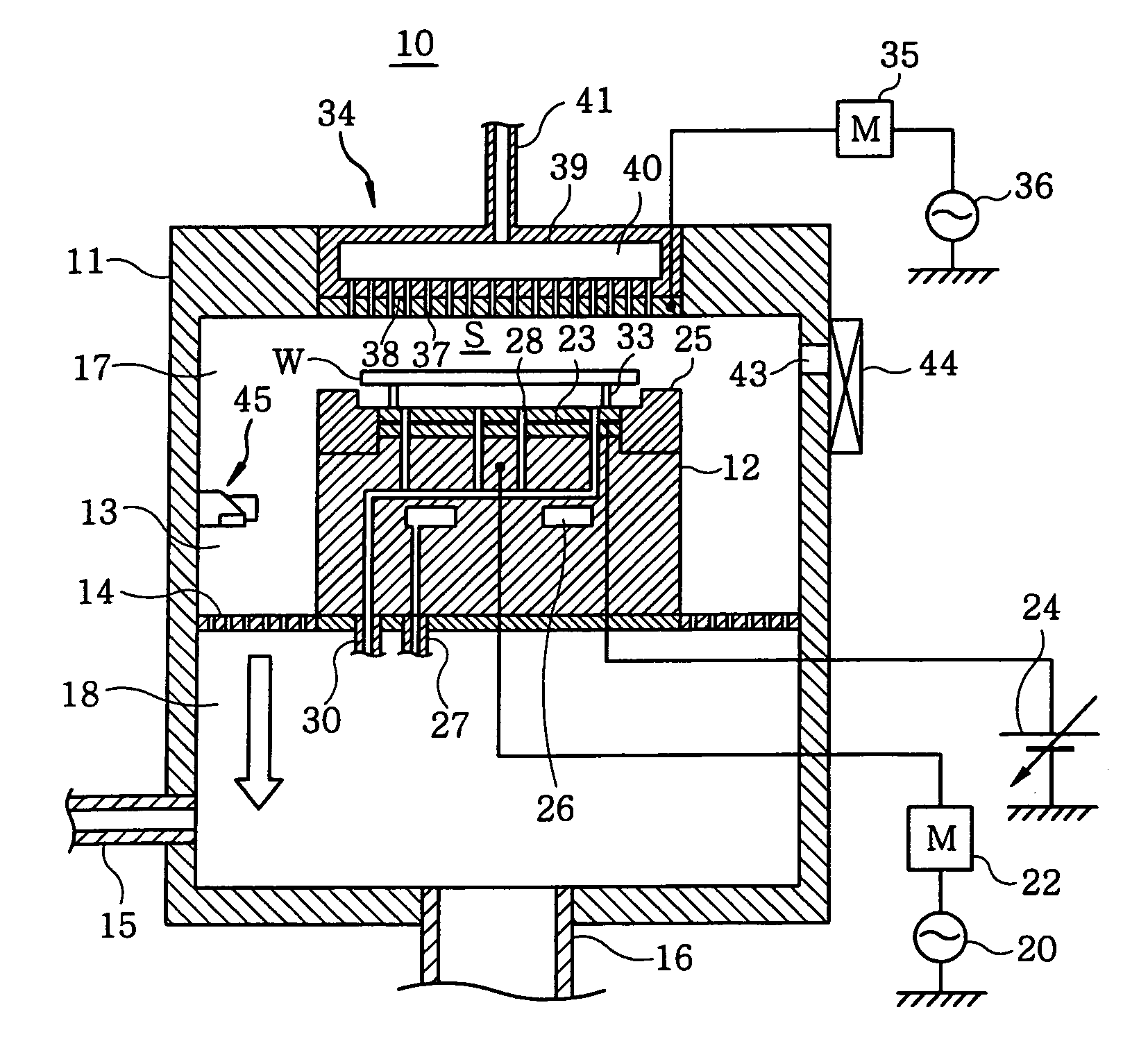
[0058]FIG. 1 is a schematic cross sectional view of the plasma processing chamber 10 in accordance with the first preferred embodiment of the present invention. The plasma processing chamber 10 is configured to perform a RIE (reactive ion etching) process on a semiconductor wafer serving as a substrate.

[0059] The plasma processing chamber 10 of FIG. 1 includes a chamber (vessel) 11 for accommodating therein a semiconductor wafer W (hereinafter, simply referred to as “wafer”) having a diameter of 300 mm, for example. Installed in the chamber 11 is a cylindrical susceptor 12 serving as a mounting table for mounting thereon the wafer W.

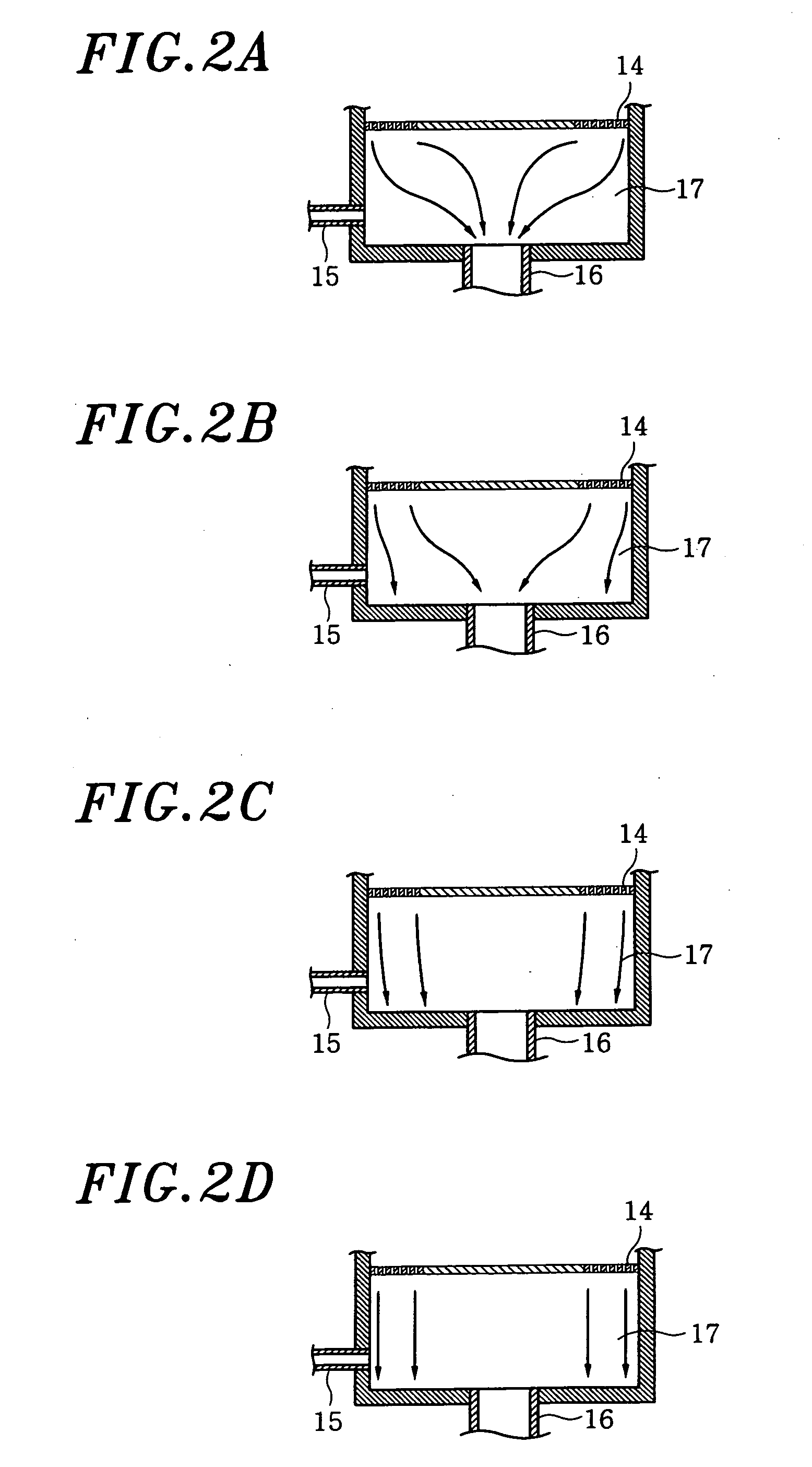
[0060] In the plasma processing chamber 10, a side exhaust passage 13 for discharging gas exi...


PUM

PropertyMeasurementUnit
pressuresaaaaaaaaaa
pressuresaaaaaaaaaa
pressuresaaaaaaaaaa

Abstract

A plasma processing chamber includes a vessel for accommodating therein a substrate; a gas supply unit for supplying a processing gas into the vessel; an electrode for applying a high frequency power into the vessel; a gas exhaust unit, connected to the vessel, for discharging gas from the vessel; and a particle detector for detecting particles floating in the vessel. The particle detector is positioned on a passage functioning as a free-fall path of the particles and also as a moving path of particles carried by the gas discharged from the vessel through the gas exhaust unit. Further, the gas exhaust unit of the plasma processing chamber has a gas exhaust port opened in the vessel toward the free-fall path of the particles.

Description

CROSS-REFERENCE TO RELATED APPLICATIONS [0001] This document claims priority to Japanese Patent Application No. 2005-288356, filed on Sep. 30, 2005 and U.S. Provisional Application No. 60 / 731,284, filed on Oct. 31, 2005, the entire content of which are hereby incorporated by reference.FIELD OF THE INVENTION [0002] The present invention relates to a plasma processing chamber having a vessel; and, more particularly, to a plasma processing chamber having a particle detector for detecting a state of particles generated in the vessel thereof. BACKGROUND OF THE INVENTION [0003] There is known a plasma processing apparatus including a chamber (vessel) serving as a vacuum processing chamber for accommodating therein a wafer as a substrate, a mounting table (susceptor) for mounting thereon the wafer accommodated in the chamber, a shower head for supplying a processing gas into the chamber, an electrode for applying a high frequency power into the chamber, and so on. [0004] In such plasma pro...

Claims


Application Information

Patent Timeline
Patent Type & Authority Applications(United States)
IPC IPC(8): H01L21/306
CPCH01J37/3244H01J37/32834H01J37/32862H01J37/32871
Inventor TSUJIMOTO, HIROSHI
Owner TOKYO ELECTRON LTD
Why Eureka
Try Eureka