Nitride based semiconductor light emitting diode

Active Publication Date: 2007-04-19
SAMSUNG ELECTRONICS CO LTD
View PDF23 Cites 55 Cited by
  • Summary
  • Abstract
  • Description
  • Claims
  • Application Information

AI Technical Summary

Benefits of technology

[0018] An advantage of the present invention is that it provides a nitride semiconductor LED in which more than three n-type electrode pads are arranged to be uniformly distributed in a large area, so that an applied high current is effectively dispersed. Therefore, it is possible to improve the current spreading efficiency and to reduce a driving voltage.
[0019] Additional aspect and advantages of the present general inventive concept will be set forth in the description which follows and, in part, will be obvious from the description, or may be learned by practice of the general inventive concept.
[0020] According to one aspect of the present invention, a nitride based semiconductor LED includes: a substrate; an n-type nitride semiconductor layer formed on the substrate, the n-type nitride semiconductor layer having the top surface divided into a first region and a second region with a finger structure, so that the first region and the second region are meshed with each other; an active layer formed on the second region of the n-type nitride semiconductor layer; a p-type nitride semiconductor layer formed on the active layer; a reflective electrode formed on the p-type nitride semiconductor laye

Problems solved by technology

Compared with the nitride based semiconductor LEDs having the vertical structure, the large-sized nitride based semiconductor LEDs having the planar structure have non-uniform current flow in an entire emissio

Method used


Image

  • Nitride based semiconductor light emitting diode
  • Nitride based semiconductor light emitting diode
  • Nitride based semiconductor light emitting diode

Examples


embodiment 1

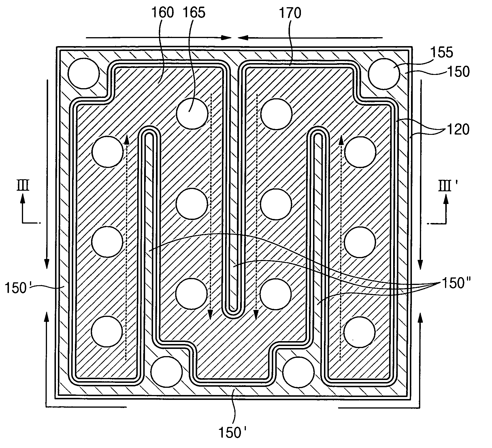
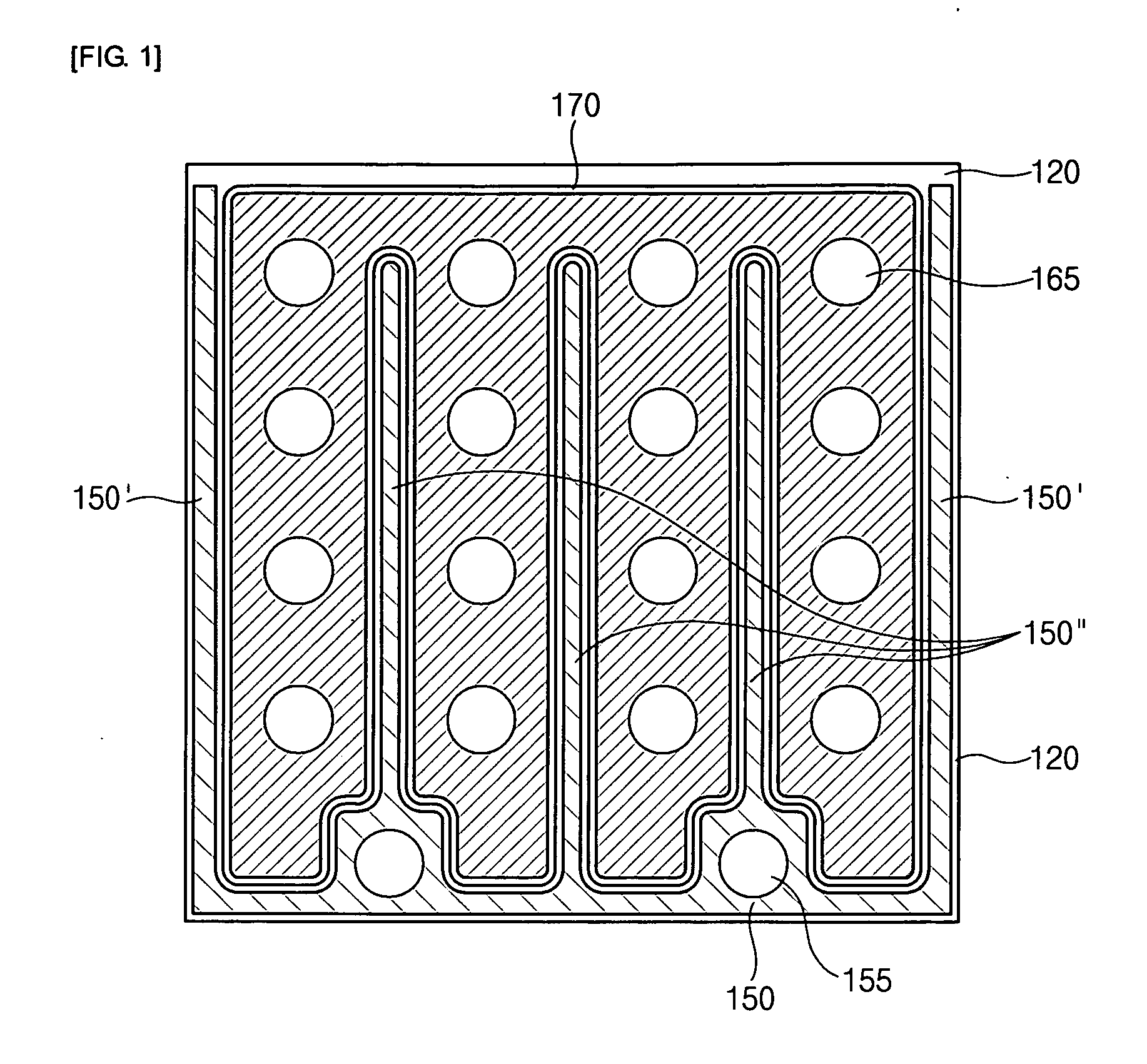
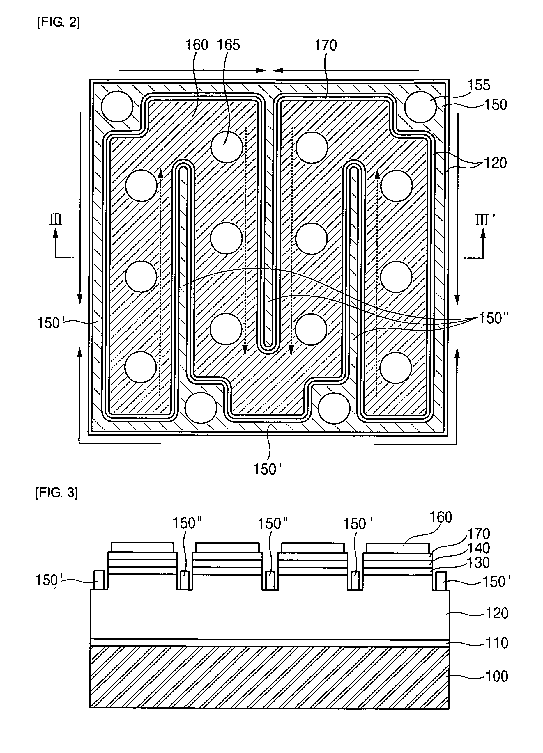
[0035] A large-sized nitride based semiconductor LED having a planar structure according to a first embodiment of the present invention will be described in detail with reference to FIGS. 2 and 3.

[0036]FIG. 2 is a plan view illustrating the arrangement of electrodes and an active region in the nitride based semiconductor LED according to the first embodiment of the present invention, and FIG. 2 is a sectional view taken along line III-III′ of FIG. 2.

[0037] Referring to FIGS. 2 and 3, a buffer layer 110 and an n-type nitride semiconductor layer 120 are sequentially formed on a light transmissive substrate 100. The n-type nitride semiconductor layer 120 is divided into a first region and a second region. The first region and the second region have a finger structure such that they are meshed with each other.

[0038] The second region defines an emission surface. Thus, it is preferable that an area of the second region is greater than that of the first region so as to improve the brig...

embodiment 2

[0054] A large-sized nitride based semiconductor LED having a planar structure according to a second embodiment of the present invention will be described in detail with reference to FIGS. 4 and 5. The same parts as the first embodiment of the preset invention will be omitted for conciseness.

[0055]FIG. 4 is a plan view illustrating the arrangement of electrodes and an active region in the nitride based semiconductor LED according to the second embodiment of the present invention, and FIG. 5 is a sectional view taken along line V-V′ of FIG. 5.

[0056] Referring to FIGS. 4 and 5, the nitride based semiconductor LED according to the second embodiment of the present invention is almost identical to the nitride based semiconductor LED according to the first embodiment of the present invention, except that a p-electrode 160 is divided into five sections by first and second n-type branch electrodes 150′ and 150″ of an n-electrode 150.

[0057] In the nitride based semiconductor LED according...


PUM


Abstract

A nitride based semiconductor LED is provided. In the nitride based semiconductor LED, an n-type nitride semiconductor layer is formed on a substrate. the n-type nitride semiconductor layer has the top surface divided into a first region and a second region with a finger structure, so that the first region and the second region are meshed with each other. An active layer is formed on the second region of the n-type nitride semiconductor layer. A p-type nitride semiconductor layer is formed on the active layer, and a reflective electrode is formed on the p-type nitride semiconductor layer. A p-electrode is formed on the reflective electrode, and an n-electrode is formed on the first region of the n-type nitride semiconductor layer. A plurality of n-type electrode pads are formed on the n-electrode. At least one of the n-type electrode pads are arranged adjacent to different sides of the n-electrode.

Description

CROSS-REFERENCE TO RELATED APPLICATIONS [0001] This application claims the benefit of Korean Patent Application No. 2005-97604 filed with the Korean Industrial Property Office on Oct. 17, 2005, the disclosure of which is incorporated herein by reference. BACKGROUND OF THE INVENTION [0002] 1. Field of the Invention [0003] The present invention relates to a nitride based semiconductor light emitting diode (LED) that can be driven at a low driving voltage by improving the current spreading efficiency. [0004] 2. Description of the Related Art [0005] Generally, nitride based semiconductors are group III-V semiconductor crystals having an empirical formula of AlXInYGa1-X-YN (0≦X≦1, 0≦Y≦1, 0≦X+Y≦1). The nitride based semiconductors are widely used as LEDs that emit short wavelength light (ranging from ultraviolet light to green light), especially a blue light. [0006] The nitride based semiconductor LEDs are formed on an insulating substrate, such as a sapphire substrate or SiC substrate, w...

Claims


Application Information

Patent Timeline
IPC IPC(8): H01L33/00H01L33/06H01L33/10H01L33/32H01L33/38
CPCH01L33/20H01L2224/05552H01L33/38H01L33/32
Inventor KO, KUN YOOHWANG, SEOK MINPARK, HYUNG JIN
Owner SAMSUNG ELECTRONICS CO LTD
Why Eureka
Try Eureka