
Forming method and forming system for insulation film

a technology of forming method and insulation film, which is applied in the direction of electrical equipment, semiconductor devices, capacitors, etc., can solve the problems of increasing gate leakage current (tunnel current), limiting the thickness of the physical film, and impurities from the gate electrode of the misfet penetration, etc., to achieve high-reliability insulation film

Inactive Publication Date: 2007-04-19
TOKYO ELECTRON LTD
View PDF5 Cites 5 Cited by
  • Summary
  • Abstract
  • Description
  • Claims
  • Application Information

AI Technical Summary

Benefits of technology

The present invention provides a method for producing an insulation film with high reliability. The method involves forming a silicon oxide film on a silicon substrate, then sequentially adding a silicon nitride film and a permittivity film on top of the oxide film. The oxide film is formed using a plasma generated by irradiating microwave from a plane antenna with plural slits, while the silicon nitride film and permittivity film are formed using a plasma generated by irradiating microwave from a plane antenna with plural slits. The resulting insulation film has a higher permittivity than the silicon oxide film and is composed of metal as the main component. The method and system provide a reliable insulation film for use in various electronic devices.

Problems solved by technology

However, thinning a silicon oxide film to a couple nanometers, has problems such as an increase of the gate leakage current (tunnel current), and penetration of impurities from the gate electrode of the MISFET.
Due to this, when the SiN film is applied, there is a limit to securing a sufficiently thick physical film thickness, and gaining a sufficiently thin EOT by answering to the demand of miniaturization.
However, if an organic high-permittivity film is directly formed onto the silicon oxide film, the silicon oxide film and the organic film will cause a reaction.
When the carbon content is high, reliability declines, such as the occurrence of the leakage current increasing.
In this way, hitherto, it was difficult to generate a highly reliable gate insulator having a sufficient physical thickness and a sufficiently thin EOT.

Method used


Image

  • Forming method and forming system for insulation film
  • Forming method and forming system for insulation film
  • Forming method and forming system for insulation film

Examples


Embodiment Construction

[0037] The forming method of the insulation film according to the embodiment of the present invention will be described referring to the drawings.

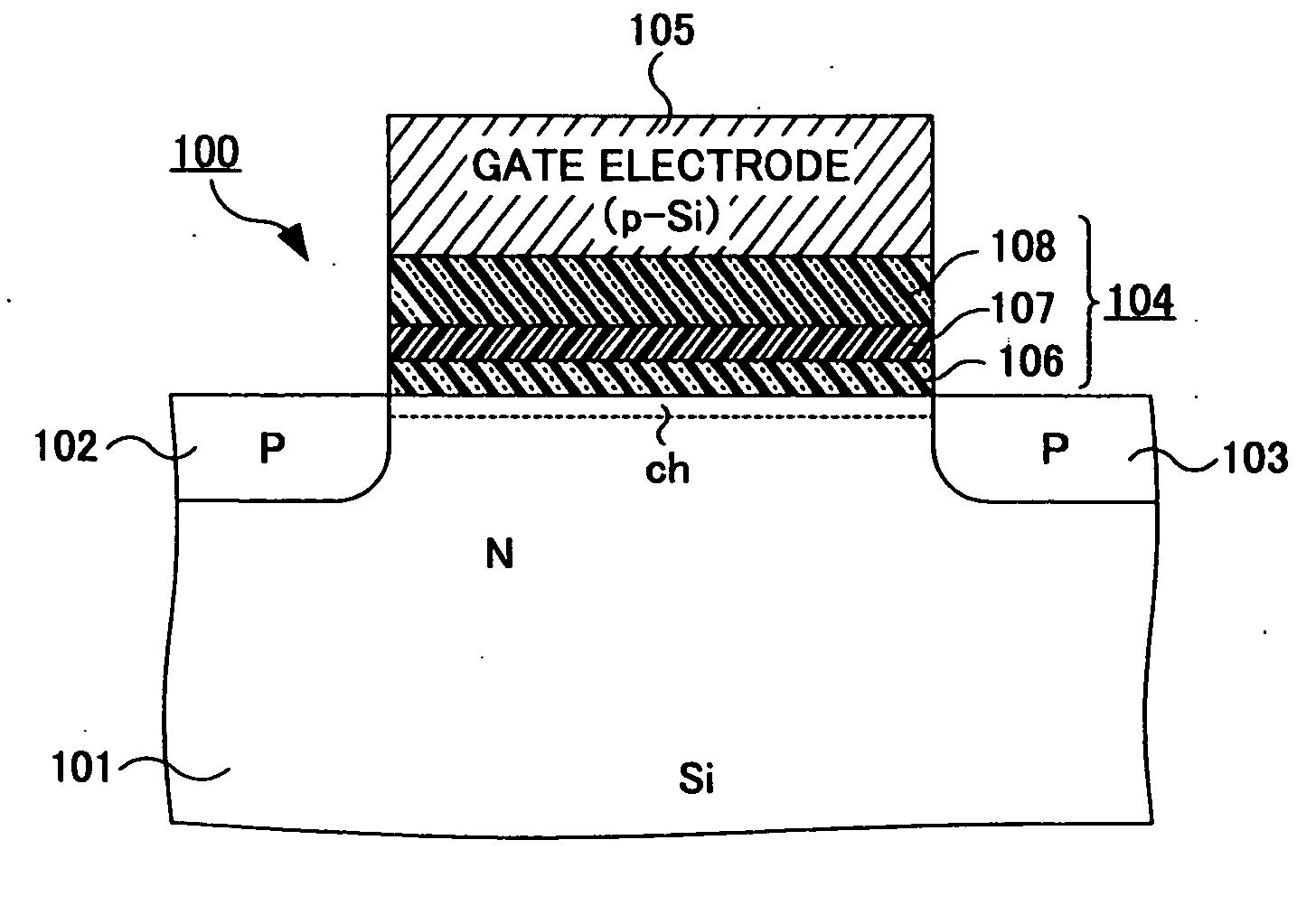
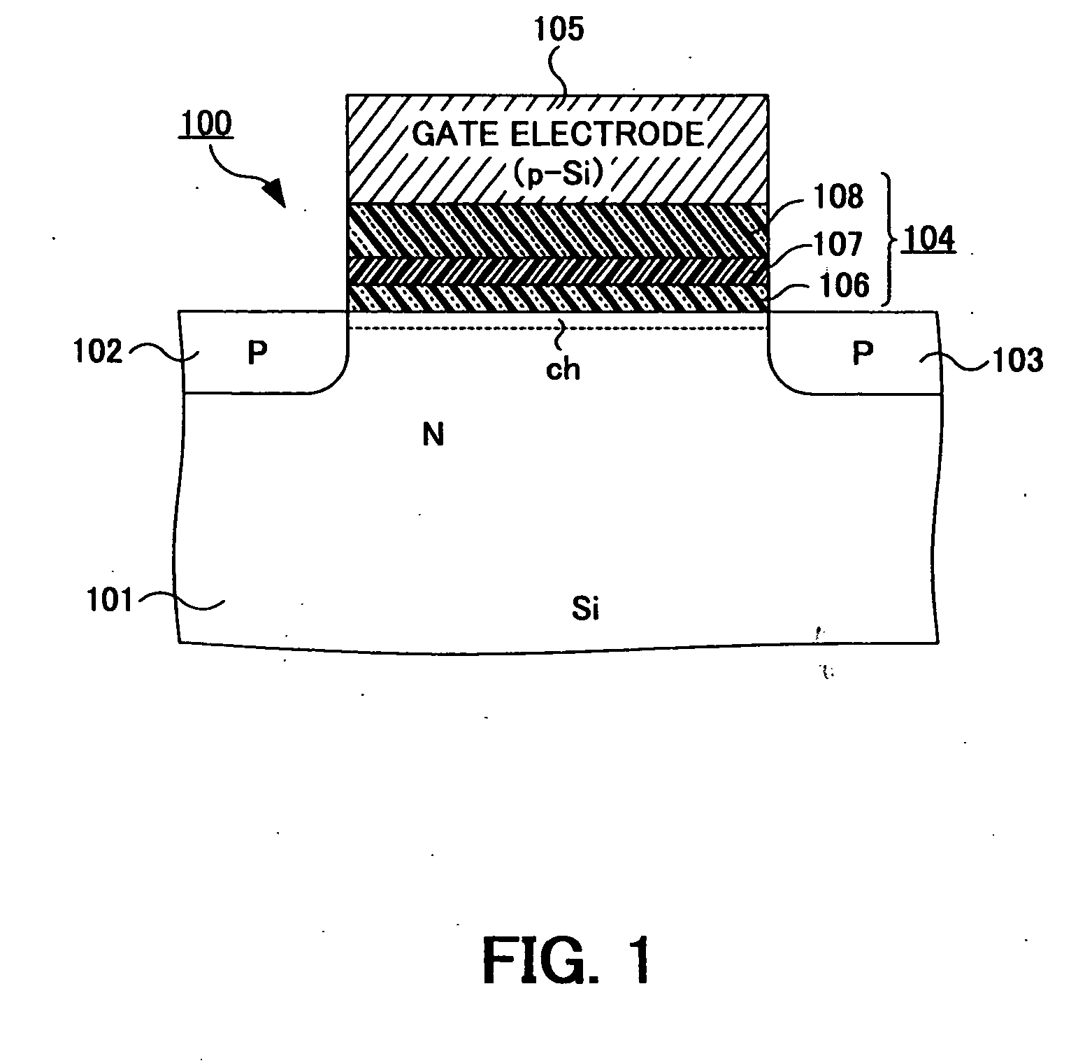
[0038] The insulation film, formed according to the embodiment of the present invention, comprises a gate insulator of a Metal Insulator Semiconductor Field Effect Transistor (MISFET) shown in FIG. 1.

[0039] As shown in FIG. 1, MISFET 100 comprises, a P-type drain region 102 and source region 103 in the surface region of an N-type silicon substrate 101, a gate insulator 104 formed on the surface region (channel region) of the silicon substrate 101, which is placed between the P-type drain region 102 and source region 103, and a gate electrode 105 formed on the gate insulator 104. Drain region 102 and source region 103, are respectively connected to a drain electrode and source electrode, comprising a MISFET 100. Silicon substrate 101, drain region 102 and source region 103, respectively may be opposite conductivity types.

[0040] On the si...


PUM

PropertyMeasurementUnit
thicknessaaaaaaaaaa
thicknessaaaaaaaaaa
thicknessaaaaaaaaaa

Abstract

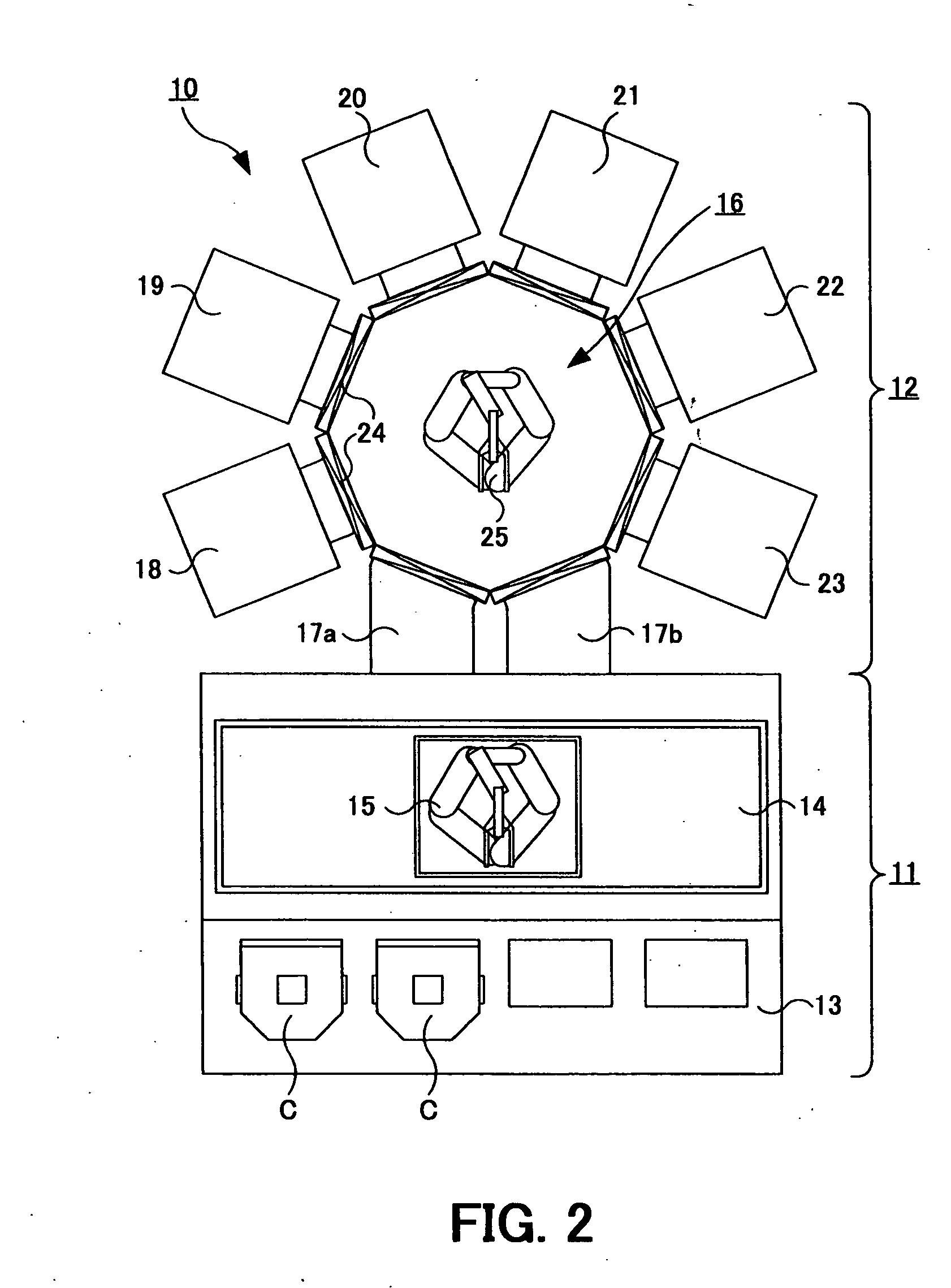
A gate insulation film (104) of a MISFET (100) is constituted of a silicon oxide film (106), silicon nitride film (107), and high-permittivity film (108). The silicon oxide film (106) and silicon nitride film (107) are formed by microwave plasma processing with a radial line slot antenna.

Description

CROSS-REFERENCE TO RELATED APPLICATIONS [0001] This application is a division of application Ser. No. 10 / 487,986, filed Feb. 27, 2004, which is the National Phase of International Application PCT / JP02 / 08735, filed Aug. 29, 2002. This application claims priority from Japanese patent application Ser. No. 2001-260179 filed Aug. 29, 2001, the entire contents of which are expressly incorporated herein by reference.TECHNICAL FIELD [0002] The present invention relates to a highly reliable forming method and forming system for insulation film. BACKGROUND ART [0003] With the high-integration and high-miniaturization of semiconductor integrated circuits, the miniaturization of Metal Insulator Semiconductor Field Effect Transistors (MISFET) on the semiconductor integrated circuits is advancing. With the miniaturization, the thickness of a gate insulator is demanded to be extremely thin, being about a couple nanometers. [0004] Generally, silicon oxide (SiO2) film, which is formed by thermal oxi...

Claims


Application Information

Patent Timeline
Patent Type & Authority Applications(United States)
IPC IPC(8): H01L21/8238H01L29/78H01L21/02H01L21/28H01L21/314H01L21/316H01L21/318H01L29/51
CPCH01L21/0214H01L21/02164H01L21/02183H01L21/022H01L21/02238H01L21/02332H01L21/28185H01L21/28194H01L21/28202H01L21/3143H01L21/31604H01L21/31612H01L21/31662H01L28/56H01L29/513H01L29/517H01L29/518Y10S438/981Y10S438/954H01L21/02252H01L21/02274H01L21/67207H01L21/67167H01J37/3222H01L21/67098H01L21/67069
Inventor MURAKAWA, SHIGEMIKUMAI, TOSHIKAZUNAKANISHI, TOSHIO
Owner TOKYO ELECTRON LTD
Learn More