Data retention in operational and sleep modes

Inactive Publication Date: 2007-04-19
ARM LTD
View PDF0 Cites 24 Cited by
  • Summary
  • Abstract
  • Description
  • Claims
  • Application Information

AI Technical Summary

Benefits of technology

[0011] The arrangement of the present invention that provides a data retention device that can retain data in sleep mode and is not itself on the forward data path, is an effective way of retaining data without slowing the critical timing path, which comprises the forward data path. Furthermore, the use of a tristateable device placed between the forward data path and the retention latch which can selectively isolate the retention latch, is a convenient way of retaining data in sleep mode and again does not effect the critical timing path. Removing these devices from the critical timing path allows the designer greater freedom in his selection of components for these devices and therefore allows for the selection of, for example, low leakage components that may not have such high performance.
[0042] As the retention latch and tristateable device are continually powered, it is highly advantageous to make them from low leakage components such as devices having a high threshold voltage. This means that there is very little static power loss from these components. Furthermore, as these components are arranged to be not on the forward data path i.e. not on the critical timing path the provision of low leakage components in this pathway does not affect the performance of the circuit.

Problems solved by technology

To enter a low leakage mode, the power transistors are turned off and the leakage of the design is limited by the leakage of the power transistors.
Although this results in substantial power savings it also results in a loss of state within the targeted circuitry.
A disadvantage of this approach is that the balloon latches consume considerable additional circuit area.
Whilst this approach reduces the increase in circuit overhead associated with providing the data retention capability, it does require control of the three clock signals of the sense amplifier flip-flops or hybrid latch flip-flops with their known disadvantages in terms of speed, power consumption and other factors.

Method used


Image

  • Data retention in operational and sleep modes
  • Data retention in operational and sleep modes
  • Data retention in operational and sleep modes

Examples


Embodiment Construction

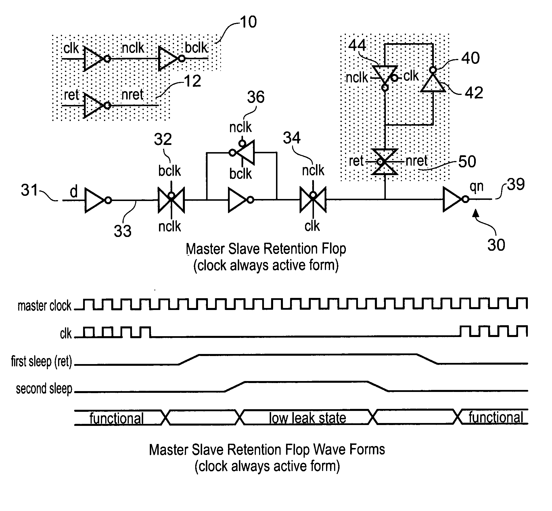
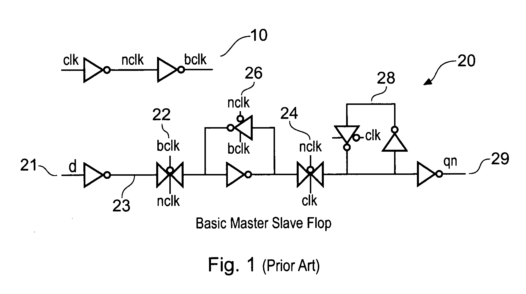
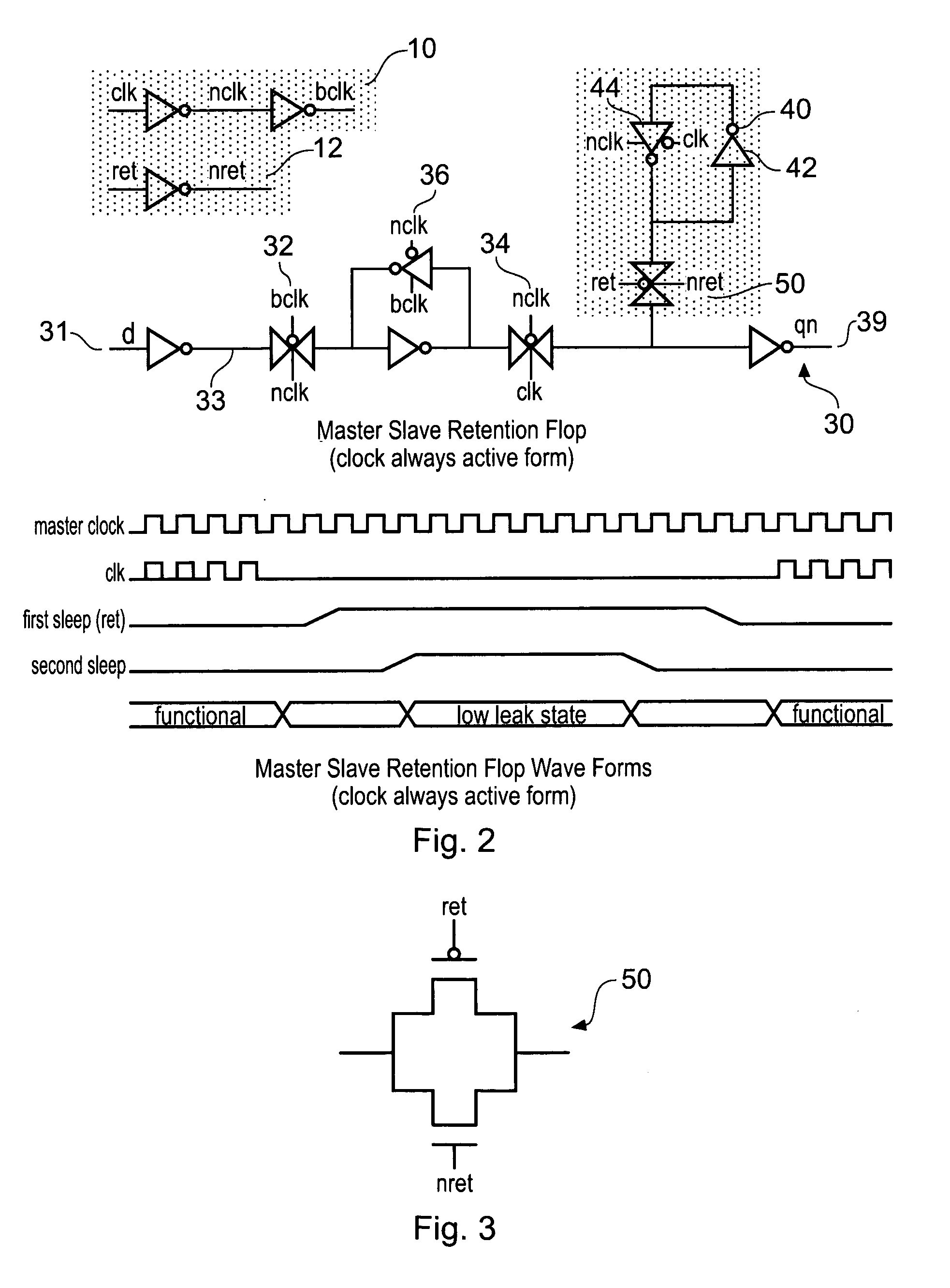
[0062]FIG. 1 shows in schematic form a basic master slave flip flop according to the prior art. This basic master slave flop 20 has a clock distribution means 10 which comprises a plurality of inverters operable to deliver different clock signals, clk, nclk an inverted form of clk, and bclk an inverted form of nclk. The basic master slave flop has a forward data path 23, between data input 21 and data output 29. This forward data path takes data from the input to a master latch 26 via transmission gate 22 and to slave latch 28 via transmission gate 24. Transmission gates 22 and 24 are tristateable devices able to provide a low impedance data path or a high impedance data path depending on the clock values at their inputs. Thus, they act to either isolate the latches or to allow transmission of data to them.

[0063]FIG. 2 shows a master slave retention flop 30 according to an embodiment of the present invention. This is an adaptation of the flop of FIG. 1 and is able to provide data r...


PUM


Abstract

A circuit is disclosed for retaining a signal value during a sleep mode while a portion of said circuit is powered down comprising: a clock signal input operable to receive a clock signal; at least one latch clocked by said clock signal; a data input, a data output and a forward data path therebetween, wherein a signal value is operable to be received at said data input, is clocked through said at least one latch and passes to said data output along said forward data path; at least one of said at least one latch comprises a retention latch operable to retain a signal value during said sleep mode, said retention latch not being located on said forward data path; and a bidirectional tristateable device, said bidirectional tristateable device being arranged between said forward data path and said retention latch and being operable to selectively isolate said retention latch from said forward data path in response to receipt of a first sleep signal; wherein in response to receipt of a second sleep signal, said second sleep signal being received after said first sleep signal, said circuit is operable to enter said sleep mode such that a voltage difference across said portion of said circuit is reduced such that said portion of said circuit is powered down, and a voltage difference across said retention latch and said bidirectional tristateable device is maintained.

Description

BACKGROUND OF THE INVENTION [0001] 1. Field of the Invention [0002] This invention relates to the field of data processing systems. More particularly, this invention relates to circuits and methods of operating circuits that allow for the storage of a signal value in both operational and sleep modes. [0003] 2. Description of the Prior Art [0004] In many circuits, particularly those that run off remote power supplies such as batteries, it is important to keep the power consumption of the circuits low. As well as addressing the issue of operational circuit efficiency attention is also being turned to reducing static power consumption, i.e. power loss due to leakage currents. One way of addressing this is to provide the circuit with a sleep mode so that it is in effect powered down during these non-operational periods. To reduce static power during these sleep periods, many circuit designs are now making use of on-chip power gating which allows rapid transitions between sleep and funct...

Claims


Application Information

Patent Timeline
IPC IPC(8): H03K3/00
CPCH03K3/356008
Inventor FREDERICK, MARLIN
Owner ARM LTD
Why Eureka
Try Eureka