

Methods for magnetically directed self assembly
- Summary
- Abstract
- Description
- Claims
- Application Information
AI Technical Summary
Benefits of technology
Problems solved by technology
Method used
Image

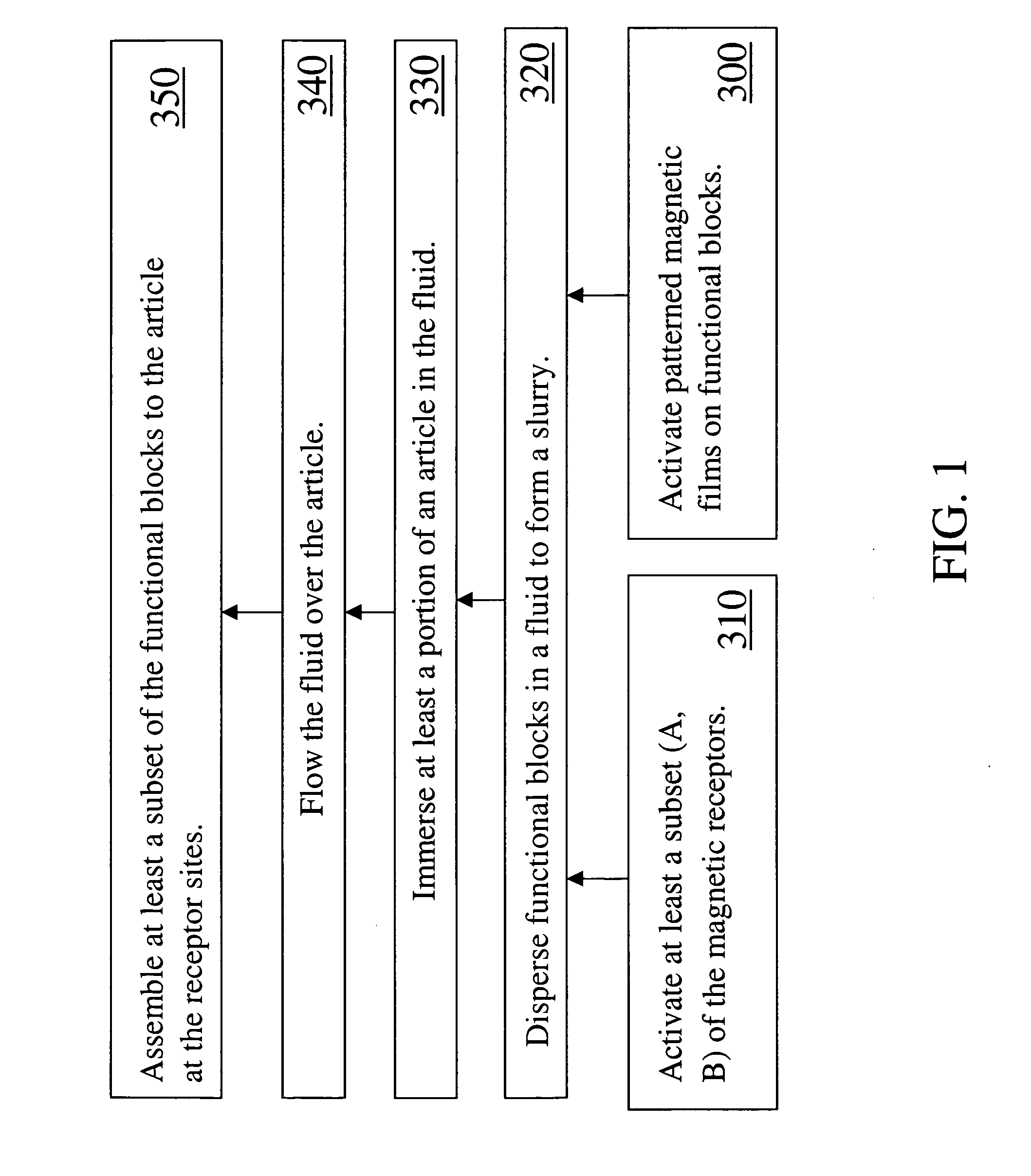
Examples
example
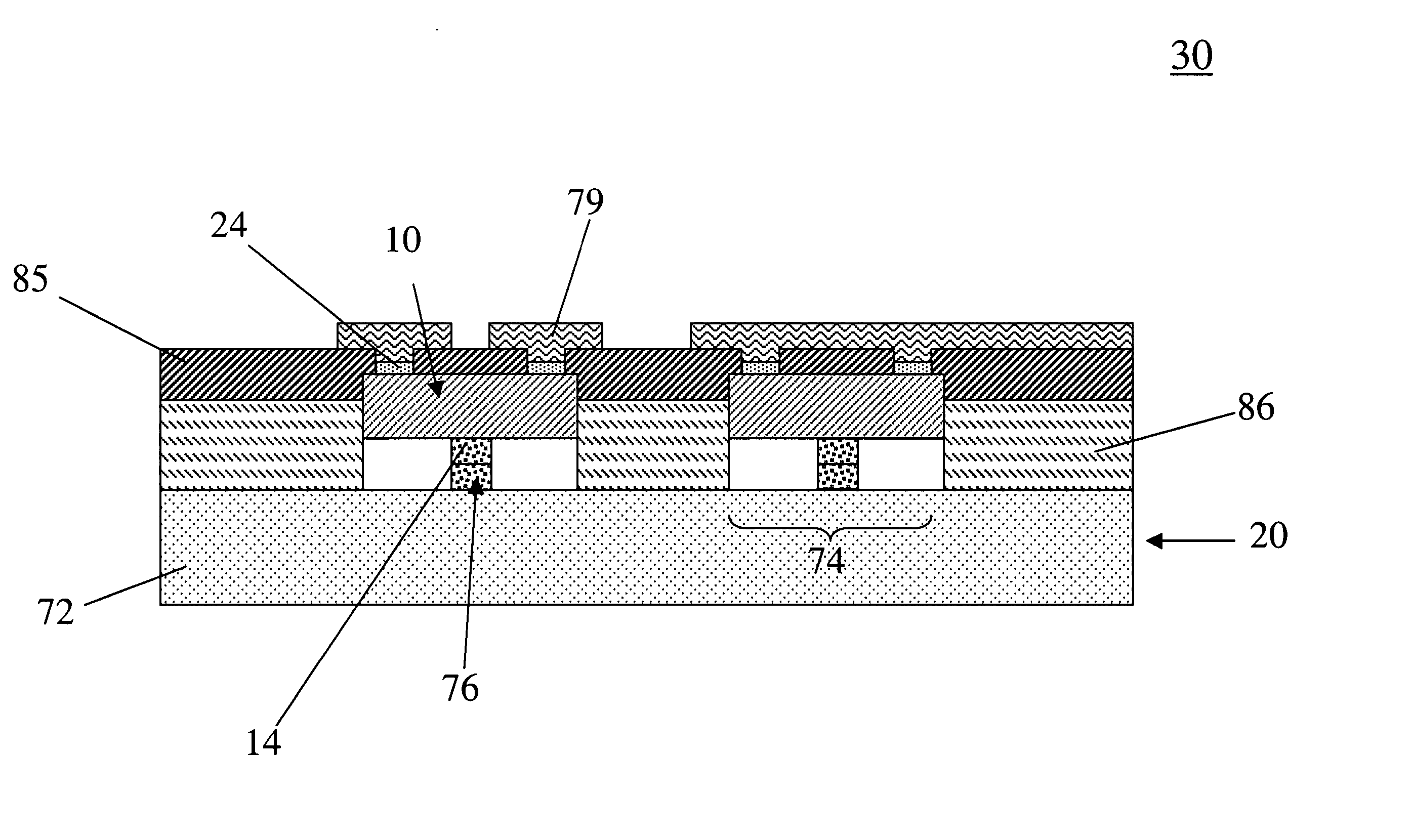
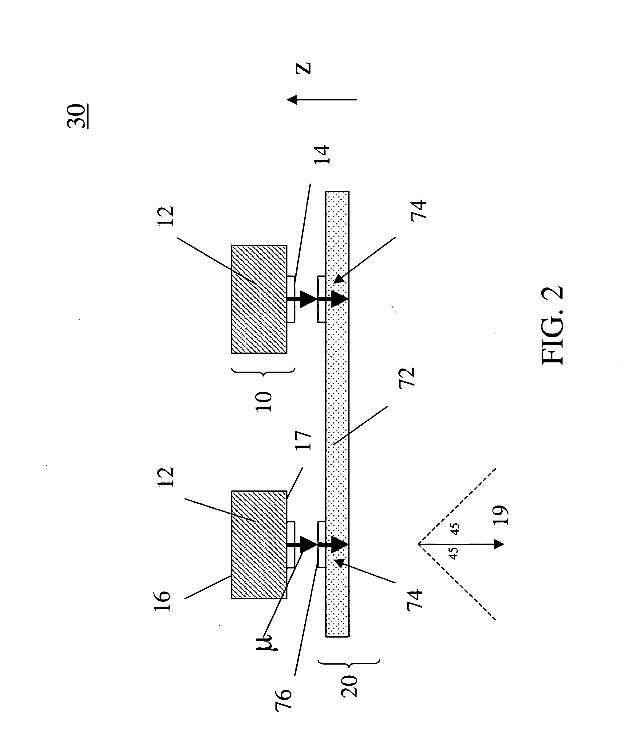
[0046] The patterned magnetic film 14 may be fabricated from a variety of different materials using a variety of different techniques. For example, a perpendicular magnetic film may be constructed as a multilayer film (also indicated by reference numeral 14). In one non-limiting example illustrated by FIG. 3, a multilayer magnetic film 14 is constructed by sequentially depositing a series of individual layers comprising a base region 14a, an active region 14b and a capping region 14c. The multilayer film 14 may be deposited using a variety of different deposition processes, non-limiting examples of which include electron beam evaporation, sputtering, resistive source evaporation and electroplating.
[0047] In one non-limiting example, a perpendicular magnetic film may be generated via electron beam evaporation of Cobalt / Platinum multilayers in the active region 14b. For the example illustrated by FIG. 3, the base region 14a comprises approximately 5.0 nm of Titanium (Ti) followed by ...
PUM
| Property | Measurement | Unit |
|---|---|---|
| Angle | aaaaa | aaaaa |
| Angle | aaaaa | aaaaa |
| Flow rate | aaaaa | aaaaa |
Abstract
Description
Claims
Application Information