Semiconductor device and method for fabricating the same

a technology of semiconductor devices and semiconductors, applied in the direction of semiconductor devices, electrical equipment, transistors, etc., to achieve the effects of high-performance semiconductor devices, reduced manufacturing costs, and improved thickness

Active Publication Date: 2007-04-26
GK BRIDGE 1
View PDF2 Cites 18 Cited by
  • Summary
  • Abstract
  • Description
  • Claims
  • Application Information

AI Technical Summary

Benefits of technology

[0037] According to the present invention, only a thickness of a stress film formed on a gate electrode is selectively increased to a larger thickness than a deposition thickness. Thus, a stress applied in a channel region can be effectively increased, compared to a known semiconductor device using a stress film, when the same deposition thickness is used in both of the known and inventive semiconductor devices. Therefore, by increasing a drain current while a deposition thickness itself of the stress film is controlled to a thickness with which contact failure is prevented, a driving power of a MISFET can be improved, so that a high performance semiconductor device can be achieved.
[0038] As has been described, the present invention relates to semiconductor devices and methods for fabricating a semiconductor device. More particularly, when the present invention is applied to a semiconductor device including a MISFET having a sidewall structure and a method for fabricating such a semiconductor device, according to the present invention, a high performance semiconductor device can be achieved by improving a driving power of a MISFET while contact failure is prevented and the present invention is very useful.

Problems solved by technology

However, in a known semiconductor device using a liner nitride film serving as a stress film or according to a method for fabricating the semiconductor device, when a liner nitride film is deposited so as to have a large thickness for the purpose of improving driving powers of MISFETs, the following problems arise.

Method used


Image

  • Semiconductor device and method for fabricating the same
  • Semiconductor device and method for fabricating the same
  • Semiconductor device and method for fabricating the same

Examples


first embodiment

[0057] Hereafter, a semiconductor device according to a first embodiment of the present invention and a method for fabricating the semiconductor device will be described. Specifically, as an example of application of the first embodiment, a semiconductor device having complementary MISFETs with a minimum gate length of 0.1 μm or less will be described in detail with reference to the accompanying drawings.

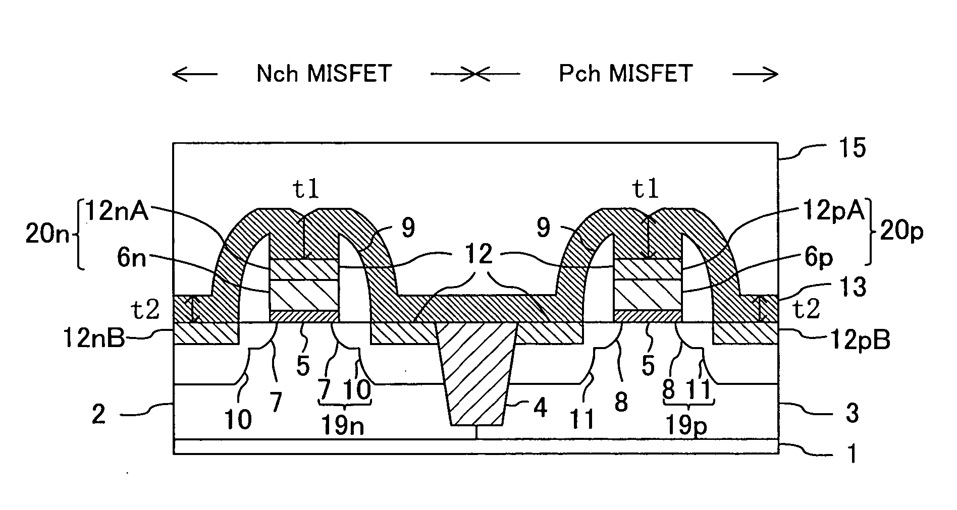
[0058]FIG. 1 is a cross-sectional view illustrating a schematic structure of a semiconductor device according to the first embodiment.

[0059] As shown in FIG. 1, the semiconductor device of this embodiment is fabricated, for example, with a p-type semiconductor substrate 1 of single crystalline silicon as a main body. The p-type semiconductor substrate 1 includes a first element formation region and a second element formation region. The first element formation region and the second element formation region are separated from each other, for example, by an insulating region for pro...

second embodiment

[0081] Hereafter, a semiconductor device according to a second embodiment of the present invention and a method of the fabricating the semiconductor device will be described. Specifically, as an example of application of the second embodiment, a semiconductor device having complementary MISFETs with a minimum gate length of 0.1 μm or less will be described in detail with reference to the accompanying drawings.

[0082]FIG. 5 is a cross-sectional view illustrating a schematic structure of a semiconductor device according to the second embodiment. In FIG. 5, each member also shown in FIG. 1 in the first embodiment is identified by the same reference numeral and therefore the description thereof will be appropriately omitted.

[0083] The second embodiment is different from the first embodiment in that, as shown in FIG. 5, as a stress film, instead of the silicon nitride film 13 for generating a tensile stress in an active region of a p-type semiconductor substrate 1 (specifically, a chann...

third embodiment

[0093] Hereafter, a semiconductor device according to a third embodiment of the present invention and a method for fabricating the semiconductor device will be described. Specifically, as an example of application of the third embodiment, a semiconductor device having complementary MISFETs with a minimum gate length of 0.1 μm or less will be described with reference to the accompanying drawings. This embodiment corresponds to a modified example of the first embodiment and an objective of this embodiment is to improve a driving power of an n-channel MISFET and suppress reduction in a driving power of a p-channel MISFET.

[0094]FIG. 7 is a cross-sectional view illustrating a schematic structure of a semiconductor device according to the third embodiment. In FIG. 7, each member also shown in FIG. 1 in the first embodiment is identified by the same reference numeral and therefore the description thereof will be appropriately omitted.

[0095] The third embodiment is different from the firs...


PUM


Abstract

A MIS transistor includes a gate electrode portion, insulating sidewalls formed on side surfaces of the gate electrode portion, source/drain regions and a stress film formed so as to cover the gate electrode portion and the source/drain regions. A height of an upper surface of the gate electrode portion is smaller than a height of an upper edge of each of the insulating sidewalls. A thickness of first part of the stress film located on the gate electrode portion is larger than a thickness of second part of the stress film located on the source/drain regions.

Description

BACKGROUND OF THE INVENTION [0001] 1 Field of the Invention [0002] The present invention relates to a semiconductor device and a method for fabricating the semiconductor device, and more particularly relates to an effective technique in application to a semiconductor device including a MISFET having a sidewall structure and a method for fabricating the semiconductor device. [0003] 2. Description of Prior Art [0004] As a field-effect transistor mounted in a semiconductor device, an insulating gate type field-effect transistor called MISFET (metal insulator semiconductor field-effect transistor) has been known. This type of MISFETs is characterized in that the degree of integration can be easily increased, and therefore has been widely used as a circuit element constituting an integrated circuit to contribute to acceleration recent reduction in device size. However, with reduction in device size, different kinds of problems regarding MISFETs have come to the surface. One of the proble...

Claims


Application Information

Patent Timeline
Patent Type & Authority Applications(United States)
IPC IPC(8): H01L29/45
CPCH01L21/823807H01L21/823814H01L29/665H01L29/66545H01L29/6659H01L29/7833H01L29/7843
Inventor SEBE, AKIOKOTANI, NAOKITAKEOKA, SHINJIOKAZAKI, GENHIRASE, JUNJIAIDA, KAZUHIKO
Owner GK BRIDGE 1
Why Eureka
Try Eureka