Imprinting method and imprinting apparatus

a printing method and printing apparatus technology, applied in the direction of photomechanical apparatus, instruments, semiconductor/solid-state device details, etc., can solve the problems of high frequency noise generated when an electrical potential falls, reduced wiring density, and reduced throughput, so as to improve throughput and improve positioning precision

a printing method and printing apparatus technology, applied in the direction of photomechanical apparatus, instruments, semiconductor/solid-state device details, etc., can solve the problems of high frequency noise generated when an electrical potential falls, reduced wiring density, and reduced throughput, so as to improve throughput and improve positioning precision

US20070093079A1Inactive Publication Date: 2007-04-26TOKYO ELECTRON LTD

Image

  • Imprinting method and imprinting apparatus
  • Imprinting method and imprinting apparatus
  • Imprinting method and imprinting apparatus

Examples


first embodiment

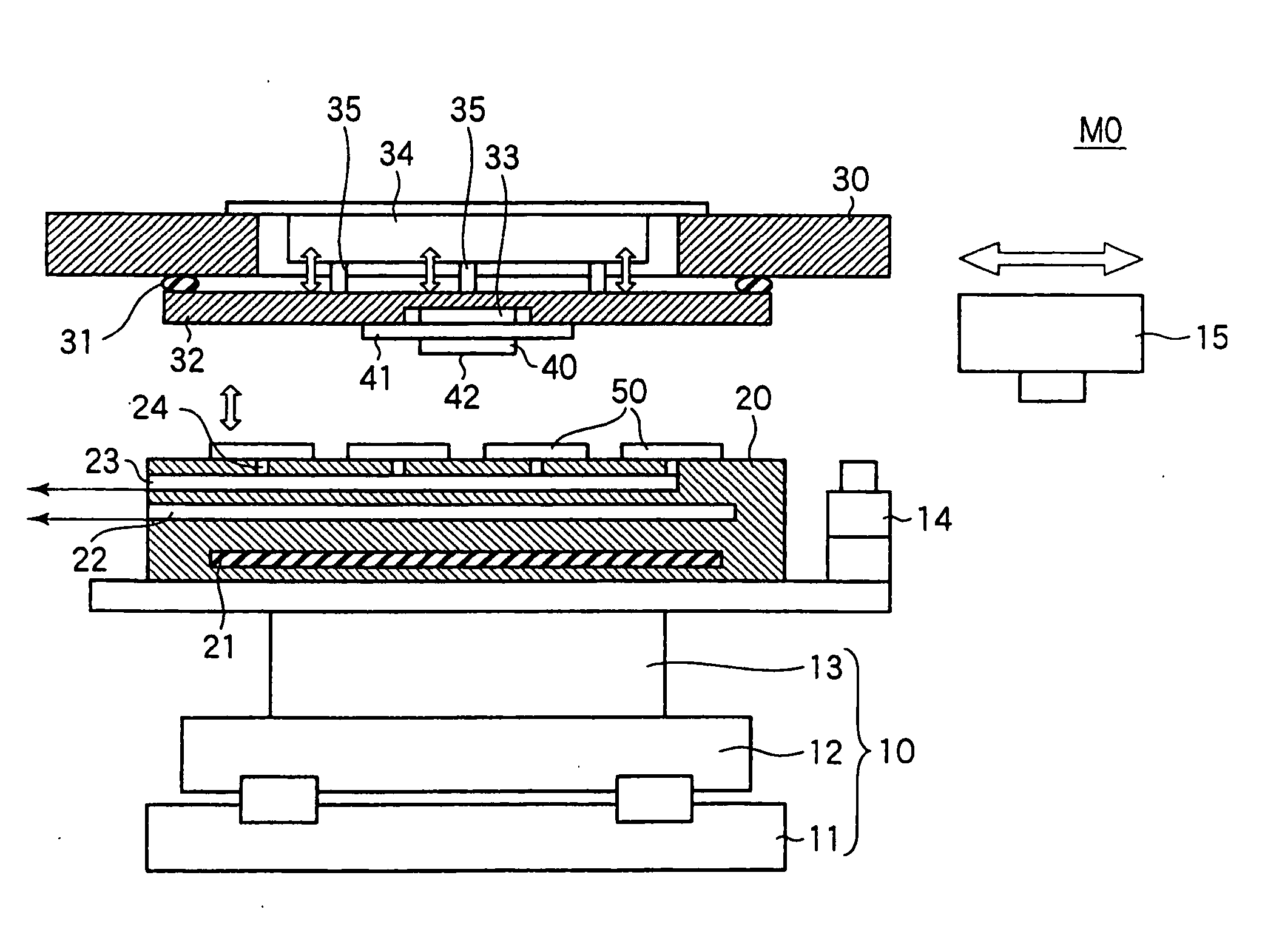
[0042] the present invention is initially described referring to FIGS. 1 to 4.

[0043] An imprinting apparatus M0 in the first embodiment shown in FIG. 1 includes a positioning mechanism 10. The positioning mechanism 10 is provided with a Y-axis table 11, an X-axis table 12, and a Z-axis table 13, which are stacked in a vertical direction. The Y-axis table 11 and the X-axis table 12 are moved in a horizontal plane in directions perpendicular to each other. The Z-axis table 13 disposed on the Y-axis table 11 and the X-axis table 12 is moved upward and downward.

[0044] A chuck stage (holding table) 20 is disposed on the positioning mechanism 10. The chuck stage 20 is capable of rotating about the Z-axis in a θ rotational direction. Displacement of the chuck stage 20 in the horizontal plane is controlled by displacement of the Y-axis table 11 and the X-axis table 12 of the positioning mechanism 10, while displacement of the chuck stage 20 in the vertical direction is controlled by displa...


PUM

PropertyMeasurementUnit
temperatureaaaaaaaaaa
pressing forceaaaaaaaaaa

Abstract

An imprinting method of the present invention is to press a mold member (40) having thereon a mold pattern onto a film carried on a principal plane of a substrate (50) as an object to be processed, so as to transfer the mold pattern to the film. A plurality of substrates (50) are fixed on a chuck stage (20). One of the substrates (50) can be selectively heated by a heater (21) and a cooling line (22). The mold member (40) is fixed on a head plate (30) which is disposed to be opposed to the chuck stage (20). The selectively heated substrate (50) and the mold member (40) are positioned relative to each other, and the mold member (40) is pressed onto a film on the substrate (50). By repeating this operation, all the substrates (50) are imprinted.

Description

TECHNICAL FIELD [0001] The present invention relates to an imprinting method and an imprinting apparatus for use in manufacturing, e.g., a semiconductor device, in which a mold member having thereon a mold pattern, such as a circuit pattern, is pressed onto a film carried on a principal plane of an object to be processed, whereby the mold pattern is transferred to the film. BACKGROUND ART [0002] In fabrication of a semiconductor device, a packaging structure, such as a system-in package (SiP) that contains a plurality of chips and passive elements of different functions, has been proposed. When a bonding wire is used in such a small-sized, high-density packaging structure to connect chips or to connect a chip to a wiring substrate, such as an interposer, the packaging structure suffers the following drawback. That is, a high frequency noise is generated when an electrical potential falls upon switching, because of a large mechanical impact on the chips, a limited wiring density, and...

Claims


Application Information

Patent Timeline
26 Apr 2007
Publication
US20070093079A1
IPC
H01L21/00; B44C1/22; B29C47/00; E04G11/22; H01L23/12; G03F7/00; G03F9/00; H01L21/48; H01L21/56; H01L23/32
CPC
B82Y10/00; B82Y40/00; G03F7/0002; G03F9/00; H01L21/4803; H01L21/563; H01L21/67109; H01L2224/73203
Inventors
ARUGA, TSUYOSHI; HAGIHARA, JUNICHI