Integrated circuit using complementary junction field effect transistor and MOS transistor in silicon and silicon alloys

a junction field effect transistor and complementary technology, applied in the field of integrated circuits and devices, can solve the problems of limited current drive and limited maximum power supply voltage of jfets, and achieve the effect of reducing the power supply voltage of the jfets to below the diode drop

Inactive Publication Date: 2007-05-03
MIE FUJITSU SEMICON
View PDF20 Cites 65 Cited by
  • Summary
  • Abstract
  • Description
  • Claims
  • Application Information

AI Technical Summary

Benefits of technology

[0021] This invention describes a method of building complementary logic circuits using Junction Field Effect T...

Problems solved by technology

The limitation of traditional enhancement mode JFET devices is that their current drive is limited by the maximum gate voltage, which is less than one diode drop.
A gate voltage in excess of one diode drop (the built-in potential) turns on the gate-channel diode which is a...

Method used


Image

  • Integrated circuit using complementary junction field effect transistor and MOS transistor in silicon and silicon alloys
  • Integrated circuit using complementary junction field effect transistor and MOS transistor in silicon and silicon alloys
  • Integrated circuit using complementary junction field effect transistor and MOS transistor in silicon and silicon alloys

Examples


Embodiment Construction

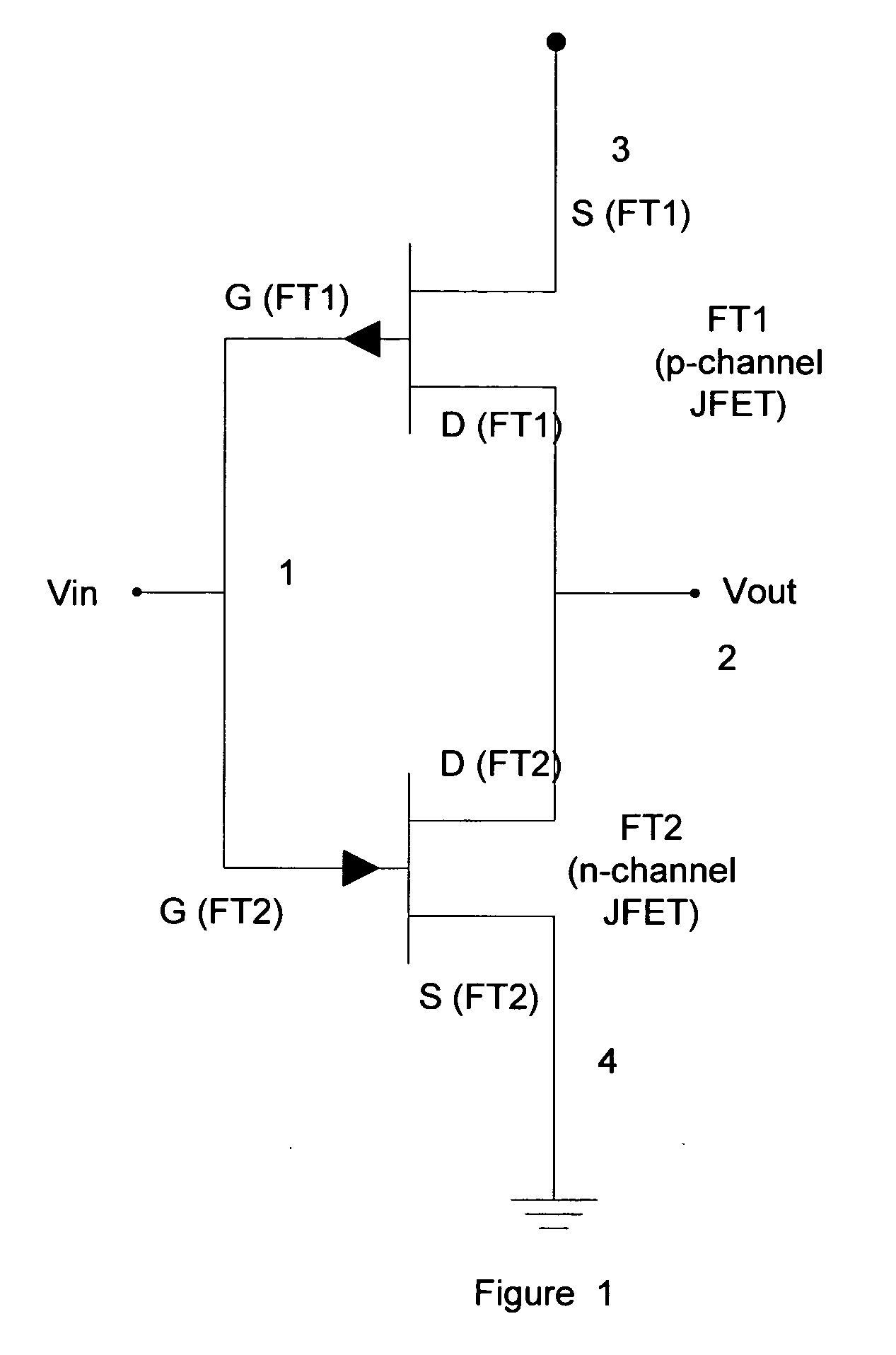
[0077] The circuit diagram of an inverter built with this invention is shown in FIG. 1. The operating terminal voltages of the two transistors under ON and OFF conditions are shown in Table 1:

TABLE 1Terminal Voltages at the CFET Gate Under ON and OFF Conditions.VinVoutFT1FT20VddONOFFVdd0OFFON

[0078] The operation of the circuit shown in FIG. 1 is remarkably similar to the operation of the corresponding CMOS circuit. The JFETs operate at voltage levels in this invention which are similar to the voltage levels of the conventional CMOS technology. The input voltage varies between 0 and Vdd. The output voltage varies between Vdd and 0 in an inverse relationship to the input voltage. Thus, for the two states of the inverter, when the applied voltage at the input terminal is 0 and Vdd, the output voltage is Vdd and zero respectively. This is achieved by the two transistors FT1 and FT2 being switched ON and OFF, as stated in Table 1 above.

[0079] As is-known to those skilled in the art, J...


PUM


Abstract

This invention describes a method of building complementary logic circuits using junction field effect transistors in silicon. This invention is ideally suited for deep submicron dimensions, preferably below 65 nm. The basis of this invention is a complementary Junction Field Effect Transistor which is operated in the enhancement mode. The speed-power performance of the JFETs becomes comparable with the CMOS devices at sub-70 nanometer dimensions. However, the maximum power supply voltage for the JFETs is still limited to below the built-in potential (a diode drop). To satisfy certain applications which require interface to an external circuit driven to higher voltage levels, this invention includes the structures and methods to build CMOS devices on the same substrate as the JFET devices.

Description

BACKGROUND [0001] 1. Field [0002] The invention relates in general to integrated circuits and devices, in particular to MOS transistors and Junction Field Effect Transistors (JFETs) and circuits. [0003] 2. Description of Related Art [0004] Very Large Scale Integrated Circuits are being scaled to smaller dimensions to gain greater packing density and faster speed in a continuation of the trend of the past thirty years. Currently, CMOS technology is being manufactured with sub-100 nanometer (nm) minimum dimensions in 2005. Scaling CMOS with the minimum line width below 100 nm presents numerous problems to designers of integrated circuits. A few of the problems of the scaled CMOS transistors below 100 nm are highlighted below; [0005] 1. Power dissipation in CMOS is a big problem due to the high switching load caused by the increase in gate capacitance per unit area as the thickness of the gate dielectric is scaled. [0006] 2. The thickness of the gate dielectric used in the MOS transist...

Claims


Application Information

Patent Timeline
IPC IPC(8): H01L31/111H01L21/337
CPCH01L21/2257H01L27/0611H01L27/098H01L29/41783H01L29/456H01L29/66492H01L29/66901H01L29/7833H01L29/808
Inventor KAPOOR, ASHOK K.
Owner MIE FUJITSU SEMICON
Why Eureka
Try Eureka