

Semiconductor device
a technology of semiconductor devices and dielectric capacitors, applied in semiconductor devices, semiconductor/solid-state device details, electrical apparatus, etc., can solve the problems of poor wire bonding, poor copper exudation prevention effect, and failure of attachment of wire bonding or degradation of pad reliability after package sealing, etc., to suppress yield reduction, suppress second wiring hardening, and prevent copper exudation more effectively
- Summary
- Abstract
- Description
- Claims
- Application Information
AI Technical Summary
Benefits of technology
Problems solved by technology
Method used
Image

Examples
first embodiment
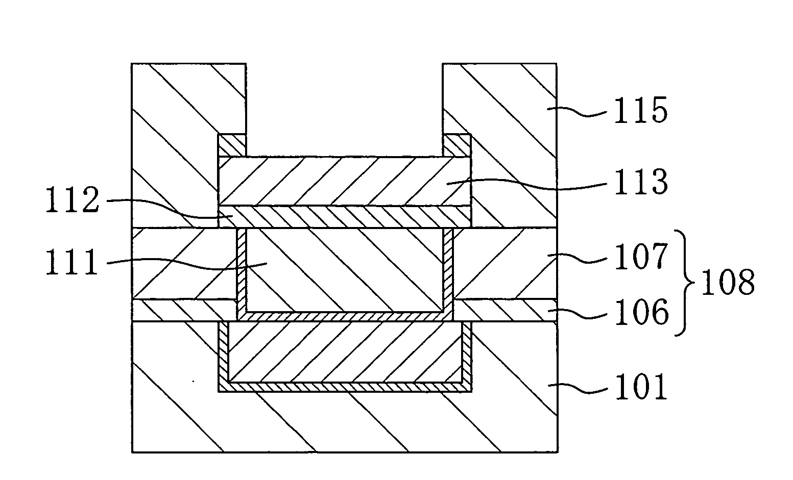
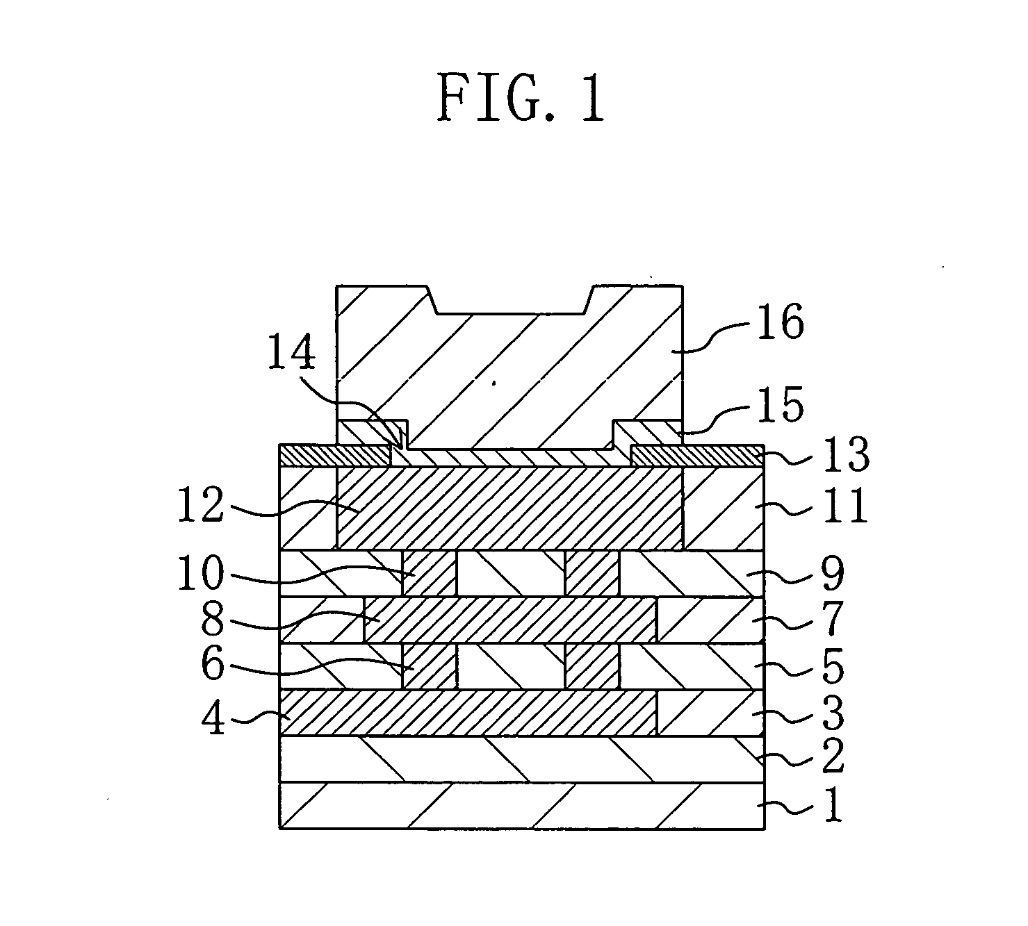
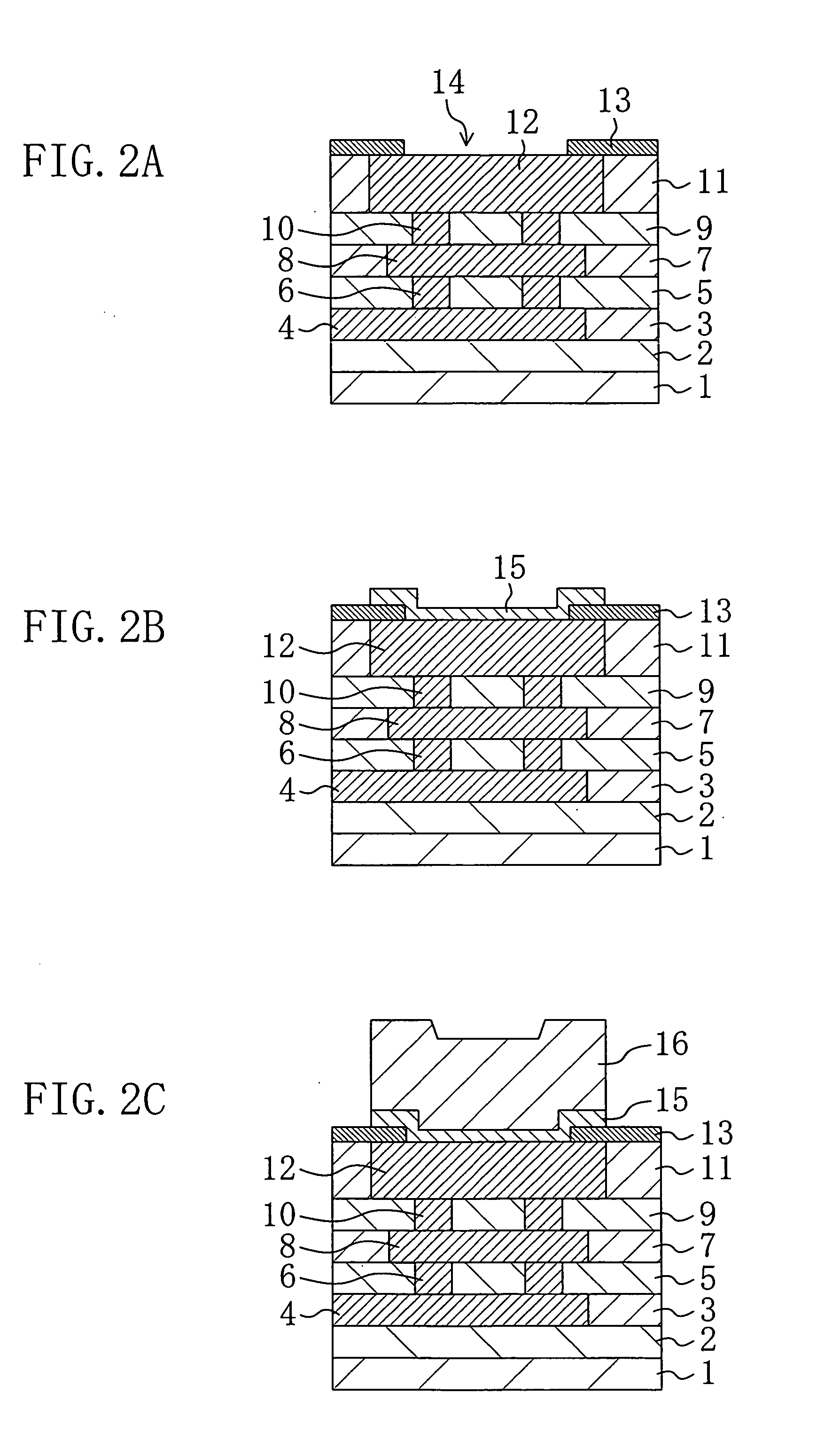
[0028] A first embodiment of the present invention will be described below with reference to the accompanying drawings. FIG. 1 is a sectional view showing the structure of a semiconductor device according to the first embodiment of the present invention. Note that FIG. 1 shows an exemplary structure in which three levels of wiring are constructed and illustration of a diffusion layer and a transistor structure is omitted.
[0029] Referring to FIG. 1, in the semiconductor device of the first embodiment, the top of a semiconductor substrate 1 of silicon with semiconductor elements (not shown) provided thereon is formed with a first insulating film 2 made of a silicon oxide film, a silicon nitride film, or the like. A second insulating film 3 of a silicon oxide film, a silicon nitride film, or the like and a first layer wiring 4 of Cu or a Cu alloy are formed on the first insulating film 2. A third insulating film 5 of a silicon oxide film, a silicon nitride film, or the like and a via ...
second embodiment
Modification of Second Embodiment
[0050] A modification of the second embodiment will be described below with reference to the accompanying drawings. The description of this modification will be made with reference to FIGS. 5 and 6 again that have been used for the explanation of the second embodiment. In this modification, the Ti barrier film 15a shown in FIG. 5 is set to have a thickness of 100 nm or more, and the TiN barrier film 15b is set to have a thickness of 10 nm or more. The other construction thereof is identical to that of the second embodiment, so that detailed description thereof will be omitted.
[0051] Next, a method for fabricating a semiconductor device according to this modification will be described. In this modification, a sputtering method is conducted in the step shown in FIG. 6B to form the Ti barrier film 15a on the passivation film 13 and a portion of the pad 12 exposed in the opening 14. The Ti barrier film 15a is made of Ti and has a thickness of 100 nm or ...
PUM
| Property | Measurement | Unit |
|---|---|---|
| thickness | aaaaa | aaaaa |
| thickness | aaaaa | aaaaa |
| temperatures | aaaaa | aaaaa |
Abstract
Description
Claims
Application Information