Integration scheme method and structure for transistors using strained silicon

a technology of strained silicon and integrated circuits, which is applied in the field of integrated circuits, can solve the problems of difficult to remove dielectric hard masks, and often difficult to dopable polysilicon gates, etc., and achieves improved process integration, high device yield per wafer, and convenient use

Active Publication Date: 2007-05-03
SEMICON MFG INT (SHANGHAI) CORP
View PDF6 Cites 20 Cited by
  • Summary
  • Abstract
  • Description
  • Claims
  • Application Information

AI Technical Summary

Benefits of technology

[0018] Many benefits are achieved by way of the present invention over conventional techniques. For example, the present technique provides an easy to use process that relies upon conventional technology. In some embodiments, the method provides higher device yields in dies per wafer. Additionally, the method provides a process that is compatible with conventional process technology without substantial modifications to conventional equipment and processes. Preferably, the invention provides for an improved process integration for design rules of 90 nanometers and less and / or 65 nanometers and less. Additionally, the invention provides for increased mobility of holes using a strained silicon structure for CMOS devices. In a preferred embodiment, the present invention provides an improved integration scheme for CMOS devices according to an embodiment of the present invention. Depending upon the embodiment, one or more of these benefits may be achieved. These and other benefits will be described in more throughout the present specification and more particularly below.

Problems solved by technology

The dielectric hard mask is often difficult to remove and leads to undesirably eroding the polysilicon gate spacer, which has been formed after the polysilicon gate patterning process as well as the shallow trench isolation (STI) process.
Doping of the polysilicon gate is often difficult and leads to other limitations.

Method used


Image

  • Integration scheme method and structure for transistors using strained silicon
  • Integration scheme method and structure for transistors using strained silicon
  • Integration scheme method and structure for transistors using strained silicon

Examples


Embodiment Construction

[0022] According to the present invention, techniques for processing integrated circuits for the manufacture of semiconductor devices are provided. More particularly, the invention provides a method and structures for integrating PMOS and NMOS devices using strained silicon structures for advanced CMOS integrated circuit devices. But it would be recognized that the invention has a much broader range of applicability.

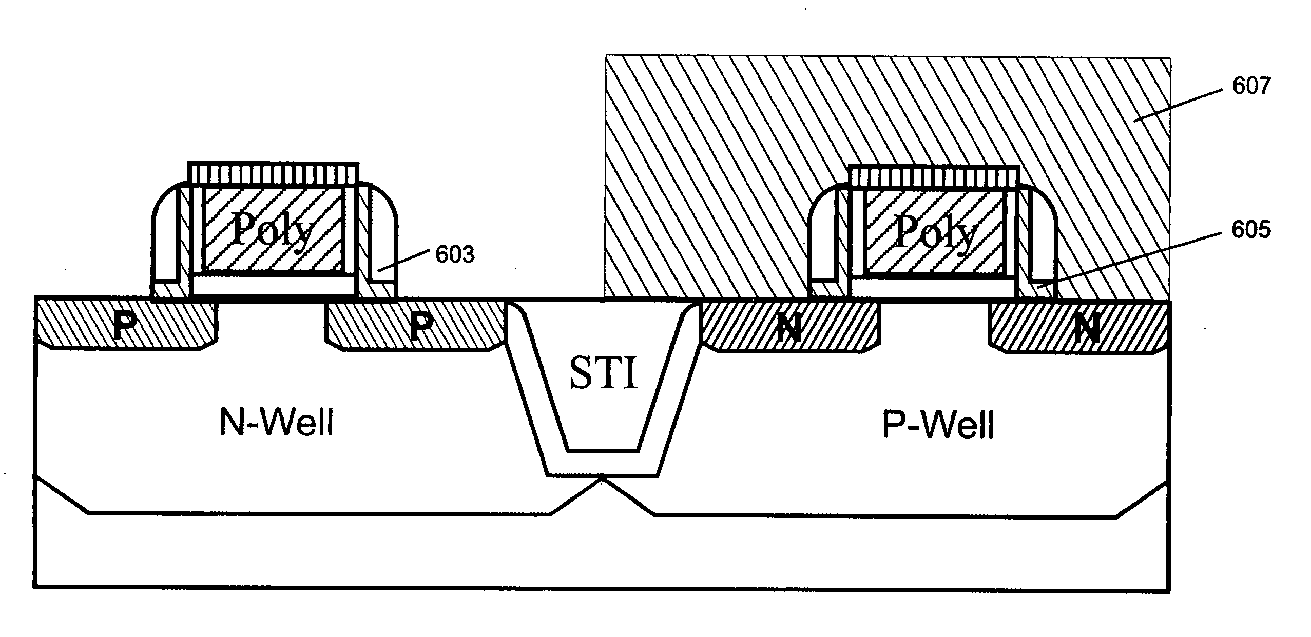
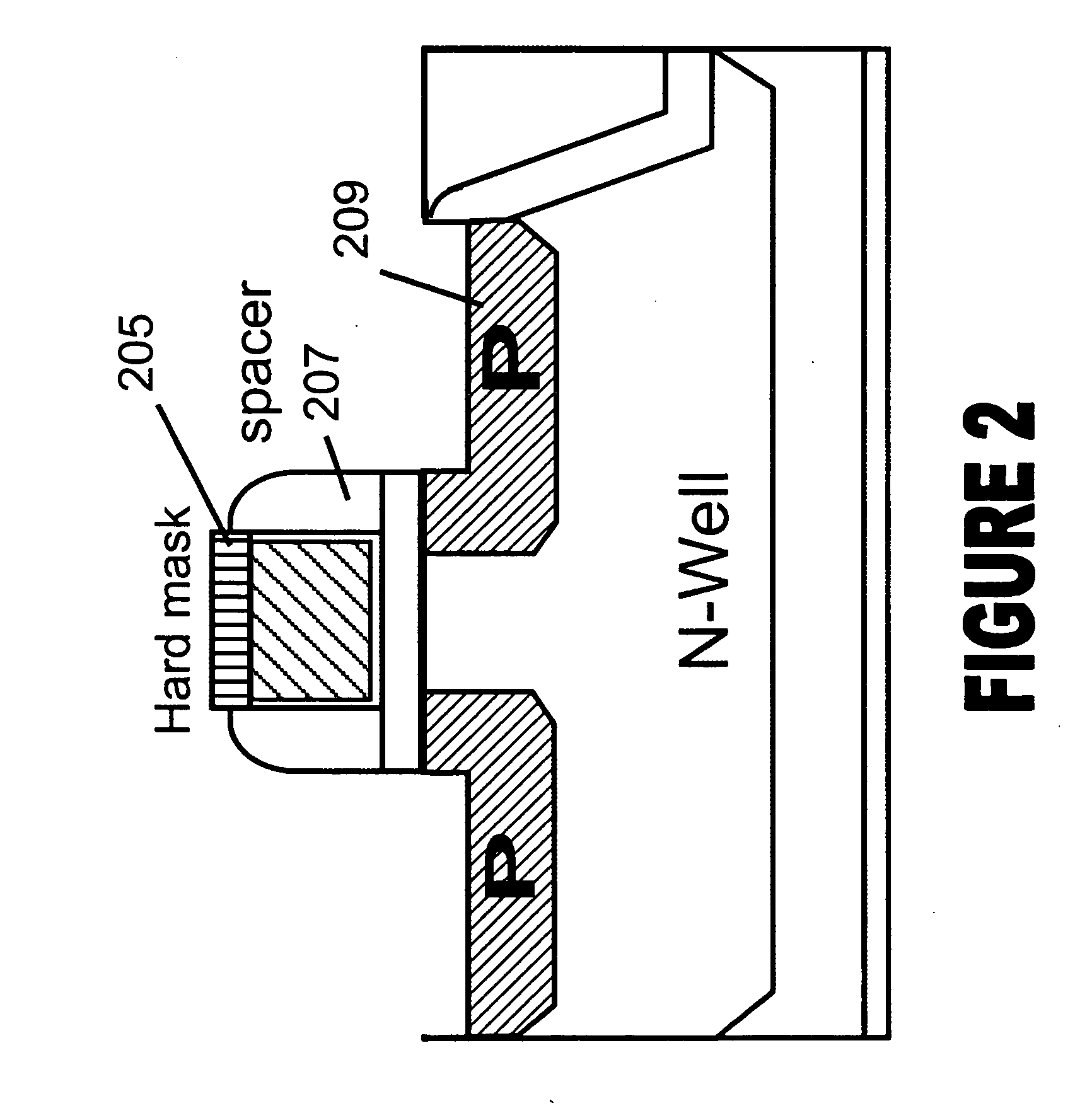
[0023]FIGS. 1 through 3 are simplified cross-sectional view diagram of conventional methods for fabricating a strained silicon MOS device. Referring to FIGS. 1 through 3, a conventional process sequence has been reproduced below.

[0024] 1. Provide a silicon substrate (100);

[0025] 2. Form gate layer (103);

[0026] 3. Form dielectric hard mask (205);

[0027] 4. Pattern dielectric mask;

[0028] 5. Pattern gate layer to form polysilicon gates;

[0029] 6. Deposit spacer layer and etch back to form spacer structures 207;

[0030] 7. Etch source / drain recessed regions 209 in silico...


PUM


Abstract

A method for forming CMOS integrated circuits. The method forms a blanket layer of silicon dioxide overlying an entirety of the surface region of a first well region and a second well region provided on a semiconductor substrate. The blanket layer of silicon dioxide is overlying the hard mask on the first gate structure and the second gate structure. The blanket layer of silicon dioxide is also overlying a region to be protected. Depending upon the embodiment, the region can be a sidewall spacer structure and portion of an MOS device on a peripheral region of the substrate. Of course, there can be other variations, modifications, and alternatives. The method protects the region to be protected using a masking layer, while the surface region of the first well region and the second well region being exposed. The method selectively removes exposed portions of the blanket layer of silicon dioxide, including the hard mask on the first gate structure and the second gate structure, while exposing a first polysilicon material on the first gate structure and while exposing a second polysilicon material on the second gate structure. The method strips the masking layer. The method also includes forming a silicided layer overlying the first polysilicon material on the first gate structure and the second polysilicon material on the second gate structure, while the region to be protected remains free from the silicided layer.

Description

CROSS-REFERENCES TO RELATED APPLICATIONS [0001] The present application relates to U.S. Ser. No. 11 / 244,955 (Attorney Docket No. 021653-008200US (SMIC Docket No.: I-04-160), commonly assigned, and hereby incorporated by reference for all purposes.[0002] The present application claims priority to Chinese Patent Application No. 200510110068.6 (filed Oct. 31, 2005) commonly assigned, and hereby incorporated by reference for all purposes. BACKGROUND OF THE INVENTION [0003] The present invention is directed to integrated circuits and their processing for the manufacture of semiconductor devices. More particularly, the invention provides a method and structures for integrating PMOS and NMOS devices using strained silicon structures for advanced CMOS integrated circuit devices. But it would be recognized that the invention has a much broader range of applicability. [0004] Integrated circuits have evolved from a handful of interconnected devices fabricated on a single chip of silicon to mil...

Claims


Application Information

Patent Timeline
Patent Type & Authority Applications(United States)
IPC IPC(8): H01L21/336H01L21/8238
CPCH01L21/7624H01L21/823807H01L21/823814H01L29/165H01L29/66628H01L29/66636H01L29/7848
Inventor NING, XIAN J.
Owner SEMICON MFG INT (SHANGHAI) CORP
Why Eureka
Try Eureka