Plasma etching of tapered structures

a plasma etching and tapered structure technology, applied in the field of plasma etching substrates, can solve the problems of small bond pads on devices and advanced packaging, etching passage bowing, and the size of etched structures, and achieve the effect of improving the precision of micro-sized structur

Inactive Publication Date: 2007-05-17
SCHOTT AG
View PDF23 Cites 9 Cited by
  • Summary
  • Abstract
  • Description
  • Claims
  • Application Information

AI Technical Summary

Benefits of technology

[0014] It is an object of the invention to provide a method of etching of at least...

Problems solved by technology

This increased complexity leads to smaller bond pads on devices and advanced packaging challenges.
One problem of the state of art etching methods is the bowing ...

Method used


Image

  • Plasma etching of tapered structures
  • Plasma etching of tapered structures
  • Plasma etching of tapered structures

Examples


Embodiment Construction

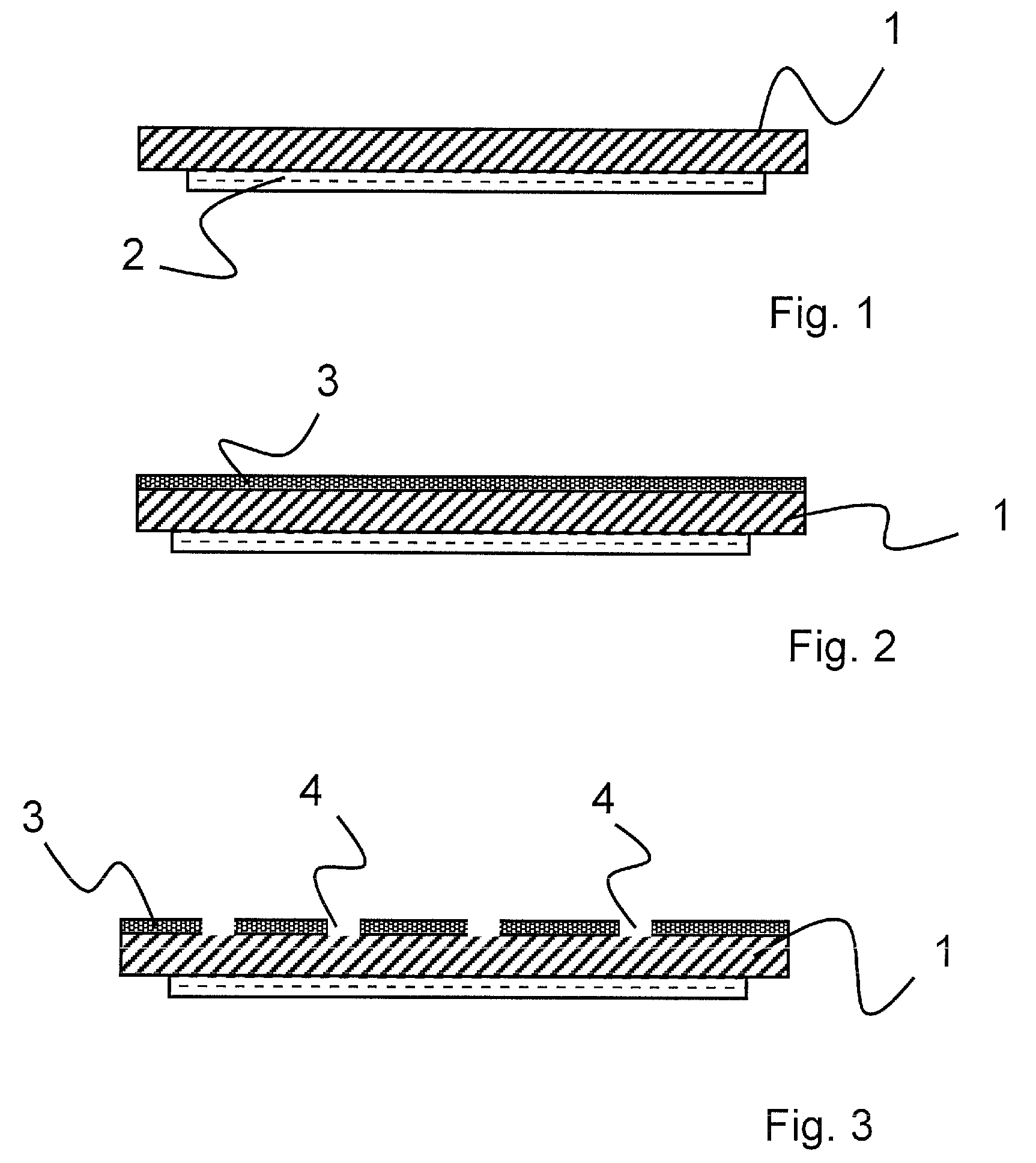
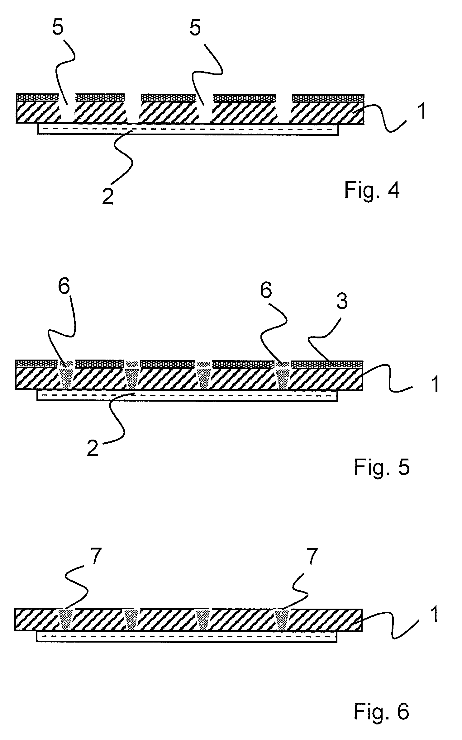
[0075]FIG. 1 to FIG. 6 show schematically the steps of etching of parts of a substrate according to an exemplary embodiment of the invention.

[0076] AS shown in FIG. 1, there is provided a substrate 1. The substrate 1 according to this embodiment of the invention is a wafer comprising electric components 2 on its front side. The electronic components 2 may comprise e.g. an image sensor or in general electronic, opto electronic, micro fluidic or micro mechanical structures.

[0077] As shown in FIG. 2, a photolithographic mask 3 is applied on the backside of the substrate 1.

[0078] As a next step according to FIG. 3, the mask 3 is structured to define openings 4 on said substrate 1. With a photolithografic arrangement or a stepper device (not shown), it is possible to apply micro sized structures with an accuracy of 10 μm or to apply sub micron sized structures with an accuracy of 0.1 μm, respectively.

[0079] Referring to FIG. 4, passages 5 are etched through the openings of the mask 3...


PUM

PropertyMeasurementUnit
Temperatureaaaaaaaaaa
Fractionaaaaaaaaaa
Fractionaaaaaaaaaa

Abstract

The invention relates to a method of plasma etching substrates, in particular of etching tapered passages through substrates, using a process gas comprising at least one halogenide and oxygen.

Description

FIELD OF THE INVENTION [0001] The invention relates to a method of plasma etching substrates, in particular micro-electronic semiconductor substrates. BACKGROUND OF THE INVENTION [0002] Plasma etching processes are commonly used to etch layers in the production of integrated circuits. Reactive Ion Etching was the main technology, but recent advanced techniques such as electron cyclotron resonance (ECR), and inductively coupled plasmas (ICP), were introduced, using magnetic fields to enhance plasma densities. [0003] It is believed that plasma etching is based in part on a chemical etching. This means that chemical reactions take place between atoms of the bulk material and gas atoms to form a molecule, which then is removed from the substrate. Due to an applied DC voltage, there also are some sputtering effects which are believed to be smaller than the chemical etching effects. Further, it is believed that the chemical etching process is increased or supported by ion bombardment. Bot...

Claims


Application Information

Patent Timeline
IPC IPC(8): C23F1/00G06F19/00
CPCH01L21/3065H01L27/14609H01L27/14634H01L27/14806H01L21/76898
Inventor NGO, HA-DUONGSEIDEMANN, VOLKERSTUDZINSKI, DANIELLANGE, MARTINHIESS, ANDRE'
Owner SCHOTT AG
Why Eureka
Try Eureka