
Magnetic impedance device, sensor apparatus using the same and method for manufacturing the same

a technology of magnetic impedance and sensor, which is applied in the direction of linear/angular speed measurement, instruments, transportation and packaging, etc., can solve the problems of deterioration of soft magnetic properties, difficult manufacturing of magnetic impedance devices, and much decreased sensitivity of devices, etc., to achieve low manufacturing cost, high heat resistance, and low sensitivity.

Inactive Publication Date: 2007-05-17
DENSO CORP
View PDF16 Cites 3 Cited by
  • Summary
  • Abstract
  • Description
  • Claims
  • Application Information

AI Technical Summary

Benefits of technology

The present invention provides a sensor apparatus with a magnetic impedance device that is small in size and made with low manufacturing cost. The magnetic impedance device has high resistance against heat treatment, and is suitable for a rotation sensor. The sensor apparatus has high mounting performance and design freedom. The invention also provides a method for manufacturing the sensor apparatus and a rotation sensor apparatus. The technical effects of the invention are to provide a sensor apparatus with improved sensitivity and high heat resistance, and to improve the accuracy of detecting the rotation of the rotation body.

Problems solved by technology

However, the magnetic impedance device with the magnetic layer made of amorphous alloy has low heat resistance, so that the sensitivity of the device is much decreased in a case where the device is processed with heat treatment above almost 400° C. The reason is as follows.
Further, in a case where the magnetic layer is formed of easily oxidizable material, the magnetic layer is oxidized with heat treatment, so that the soft magnetic property is deteriorated.
Therefore, it is difficult to manufacture the magnetic impedance device having the magnetic layer made of amorphous alloy with using a conventional semiconductor processing method.
That is because the conventional method usually includes a step of heat treatment above almost 400° C. Accordingly, it is difficult to minimize the device with using the conventional method so that the device is integrated with another circuit such as a sensor output signal processor.
Further, when the device is annealed, i.e., processed with heat treatment, a stress is generated in a substrate since thermal expansion of the substrate is different from that of the device.
However, this device is necessitated to form with limited manufacturing method and to have a limited construction.
Moreover, since a magnetic impedance device having high sensitivity is available for various sensor systems, minimization and low manufacturing cost are much required.
Therefore, minimization and reduction of manufacturing cost of the head module are limited.
That is because the magnetic impedance device has high sensitivity so that the device is easily affected by the outside disturbance of magnetic field.
However, this current sensor has a complicated construction so that a manufacturing cost is increased.

Method used


Image

  • Magnetic impedance device, sensor apparatus using the same and method for manufacturing the same
  • Magnetic impedance device, sensor apparatus using the same and method for manufacturing the same
  • Magnetic impedance device, sensor apparatus using the same and method for manufacturing the same

Examples


first embodiment

[0065] The inventors examine a magnetic thin film made of Ni—Fe series alloy as a magnetic material composing a magnetic layer in a magnetic impedance device, which has high heat resistance so that sensitivity of the device is not decreased even when the device is processed with heat treatment above 400° C.

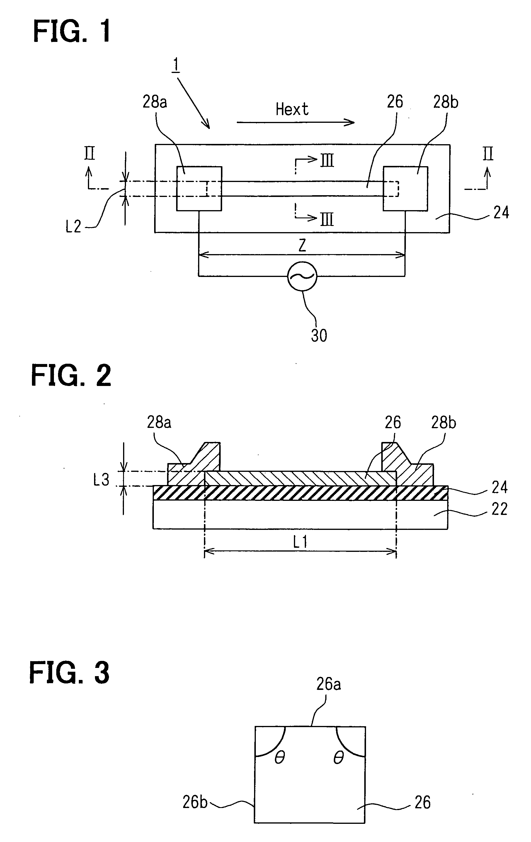
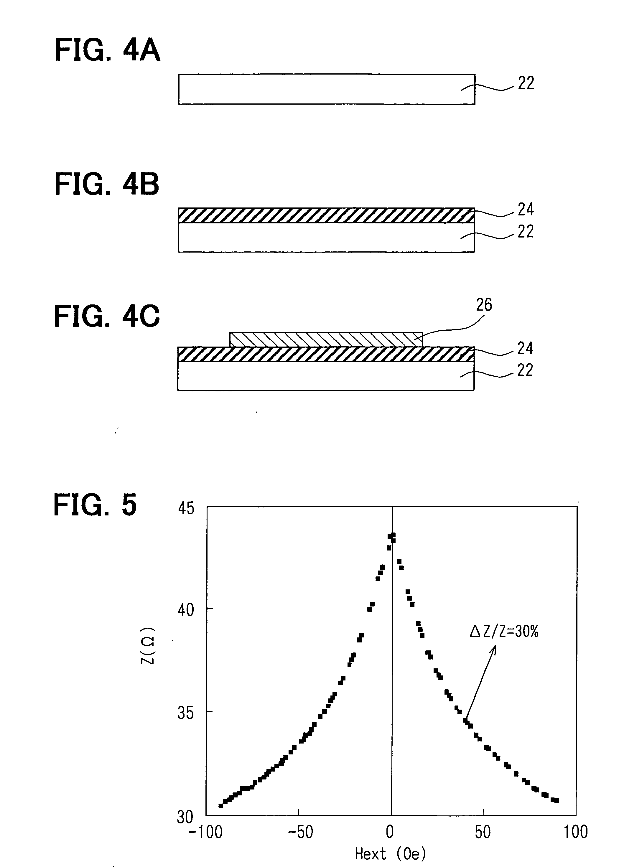
[0066] A magnetic impedance device according to a first embodiment utilizes magnetic impedance effect. The magnetic impedance effect is that impedance of the device changes in accordance with an external magnetic field when the device is energized with an alternating current. The device includes a magnetic layer made of Ni—Fe series alloy film. Here, Ni—Fe series alloy film has high Currie temperature and is made of polycrystalline. Accordingly, magnetic property of the magnetic layer made of Ni—Fe series alloy film does not change after the heat treatment above 400° C. For example, sensor sensitivity of the device is not decreased after the heat treatment. Therefore, the device ...

second embodiment

[0104] A magnetic impedance device 2 according to a second embodiment of the present invention includes the magnetic layer 26 and a protection layer 32, as shown in FIG. 19. The protection layer 32 covers the magnetic layer 26, and is made of electrically insulation material.

[0105] In general, a magnetic impedance device includes a magnetic layer having zero magneto-striction or low magneto-striction. This is because the magnetic layer having low magneto-striction is prevented from changing the magnetic properties generated by a striction of the magnetic layer, for example, from reducing the sensor sensitivity or the detection accuracy. However, the inventors obtain the following experimental results. In the device having a protection layer for covering the magnetic layer, an internal stress σ in the protection layer affects the magnetic properties of the magnetic layer, so that the sensor sensitivity is reduced. Further, there is a different influence of the internal stress σ affe...

third embodiment

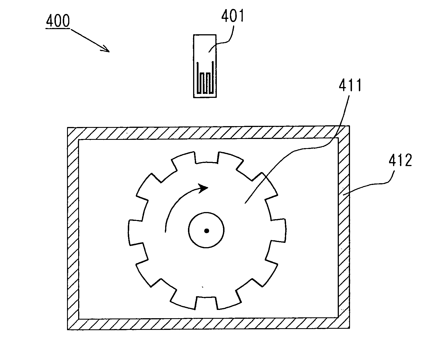
[0131] A magnetic sensor apparatus 300 having a magnetic impedance device 301 according to a third embodiment of the present invention is shown in FIGS. 25-27. FIG. 27 shows a schematic diagram of the apparatus 300. The apparatus 300 includes the magnetic impedance device 301, a resistance 312, an oscillator 313, and an amplifier 314. Here, the resistance 312, the oscillator 313 and the amplifier 314 work as a periphery circuitry. The periphery circuitry may include a regulator circuit, and an interface circuit for communicating with a signal between the apparatus 300 and an external circuit. The device 301 is made of, for example, Ni—Fe series alloy, and connects to the resistance 312 in series. Here, the device 301 made of Ni—Fe series alloy has a wide dynamic range of detection of the magnetic field with using the magnetic impedance effect. Although the device 301 according to this embodiment is made of Ni—Fe alloy, the device 301 can be formed of other materials. The resistance ...


PUM

PropertyMeasurementUnit
width L3aaaaaaaaaa
thickness L3aaaaaaaaaa

Abstract

A magnetic sensor apparatus includes a semiconductor substrate and a magnetic impedance device for detecting a magnetic field. The magnetic impedance device is disposed on the substrate. The magnetic sensor apparatus has minimum size and is made with low manufacturing cost. Here, the magnetic impedance device detects a magnetic field in such a manner that impedance of the device is changed in accordance with the magnetic filed when an alternating current is applied to the device and the impedance is measured by an external electric circuit.

Description

CROSS REFERENCE TO RELATED APPLICATIONS [0001] This application is based on Japanese Patent Applications No. 2002-337416 filed on Nov. 21, 2002, No. 2002-337417 filed on Nov. 21, 2002, No. 2003-58899 filed on Mar. 5, 2003, No. 2003-58900 filed on Mar. 5, 2003, and No. 2003-73900 filed on Mar. 18, 2003, the disclosures of which are incorporated herein by reference. FIELD OF THE INVENTION [0002] The present invention relates to a magnetic impedance device, a sensor apparatus using the same and a method for manufacturing the same. The sensor apparatus is suitably used for a rotation sensor apparatus. BACKGROUND OF THE INVENTION [0003] A conventional magnetic impedance device utilizes a magnetic impedance effect, and is disclosed in Japanese Patent Application Publication No. H08-75835. The magnetic impedance effect is that impedance of the device changes in accordance with an outside stress in a case where the device is energized with an alternating current (e.g., a high frequency alte...

Claims


Application Information

Patent Timeline
Patent Type & Authority Applications(United States)
IPC IPC(8): G01B7/30G01R33/02G01P3/487H01F10/14H10N50/10
CPCG01P3/487Y10T428/1193H01L27/22G01R33/02H10B61/00H10N59/00H10N50/10
Inventor AO, KENICHISUZUKI, YASUTOSHIYAMADERA, HIDEYAOHTA, NORIKAZUFUNAHASHI, HIROFUMI
Owner DENSO CORP
Learn More