Gate drive for lower switching noise emission

a gate drive and noise emission technology, applied in logic circuit coupling/interface arrangement, pulse generator, pulse technique, etc., can solve the problems of significant switching loss increase and harmful ringing, and achieve the effect of reducing emi, reducing switching losses, and reducing the magnitude of qrr itsel

Inactive Publication Date: 2007-05-17
INFINEON TECH AMERICAS CORP
View PDF5 Cites 24 Cited by
  • Summary
  • Abstract
  • Description
  • Claims
  • Application Information

AI Technical Summary

Benefits of technology

[0011] If three or more gate sourcing transistors are used, the transistors can be driven on in a phased sequence when VDS of the driven MOSFET begins to drop or some of these transistors can be driven on simultaneously in order to achieve the desired gate drive waveform to reduce EMI and obtain the other benefits described herein.
[0012] Considering the fact that the voltage across the body diode of the power MOSFET switch can not be reverse biased before Qrr discharges, by the time the drain-source voltage transition begins, the process of the Qrr discharge is completed. Thus, the later faster switching process can reduce switching losses without affecting the body diode discharging process which is considered to be the trigger of harmful ringing.
[0013] Another benefit of this method is that the magnitude of the Qrr itself is reduced by decreasing the di / dt by slowing down the turn-on of the MOSFET. The di / dt is usually what triggers harmful ringing. This method is effective to reduce reverse recovery charge by reducing di / dt at the turning on edge of the MOSFET, while it can still keep the same dV / dt transition time in order not to increase switching losses further.

Problems solved by technology

In a typical hard switching application, one of the main noise sources of EMI emission is di / dt spikes caused by the body diode reverse recovery charge QRR which usually has sharp waveforms and triggers harmful ringing.
One problem with this method is the effectiveness of this gate resistor is not equal to either the Qrr discharging period or transition period.
Therefore switching loss increases significantly even though reverse recovery discharging is slowed down.

Method used


Image

  • Gate drive for lower switching noise emission
  • Gate drive for lower switching noise emission
  • Gate drive for lower switching noise emission

Examples


Embodiment Construction

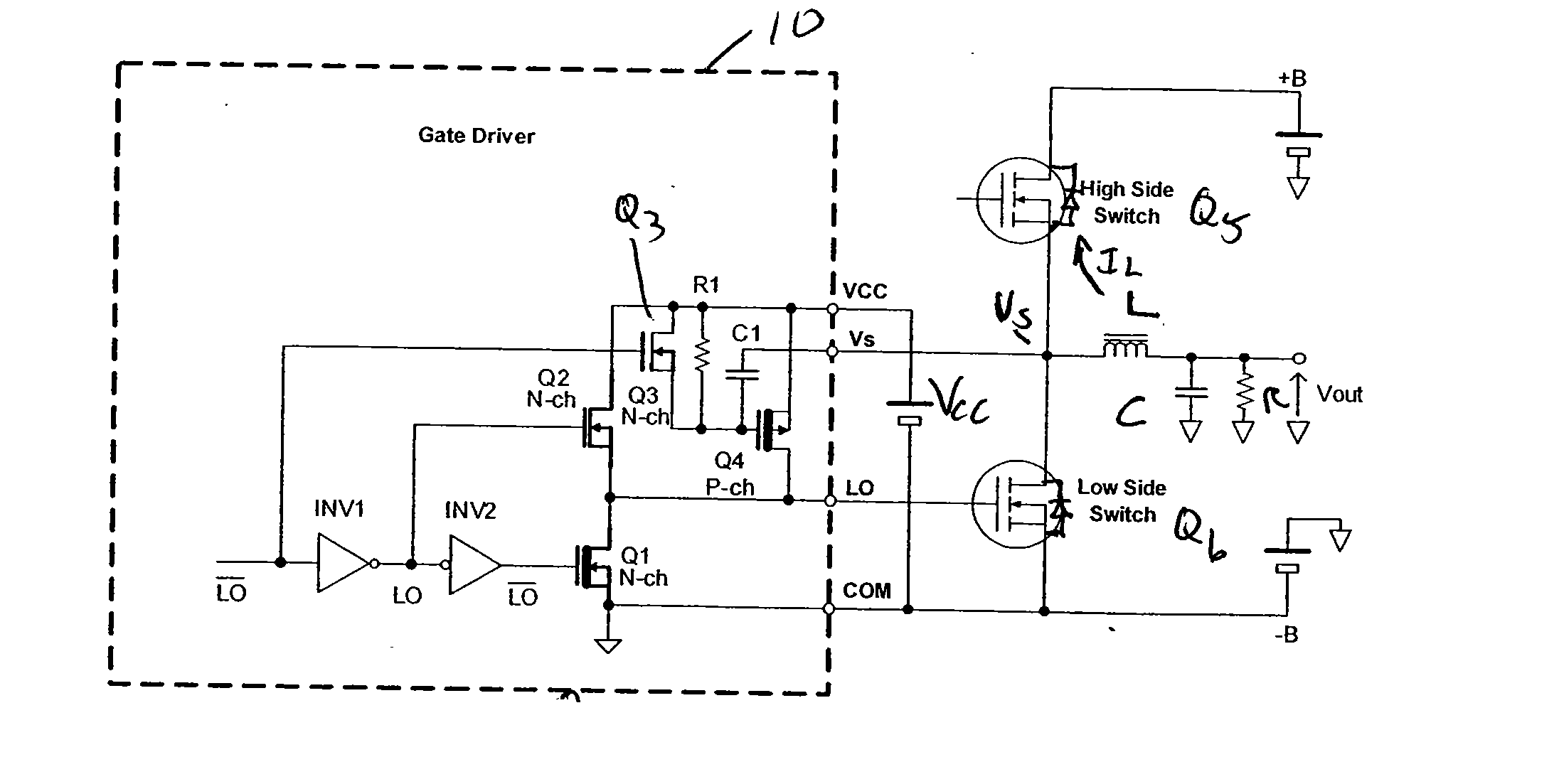
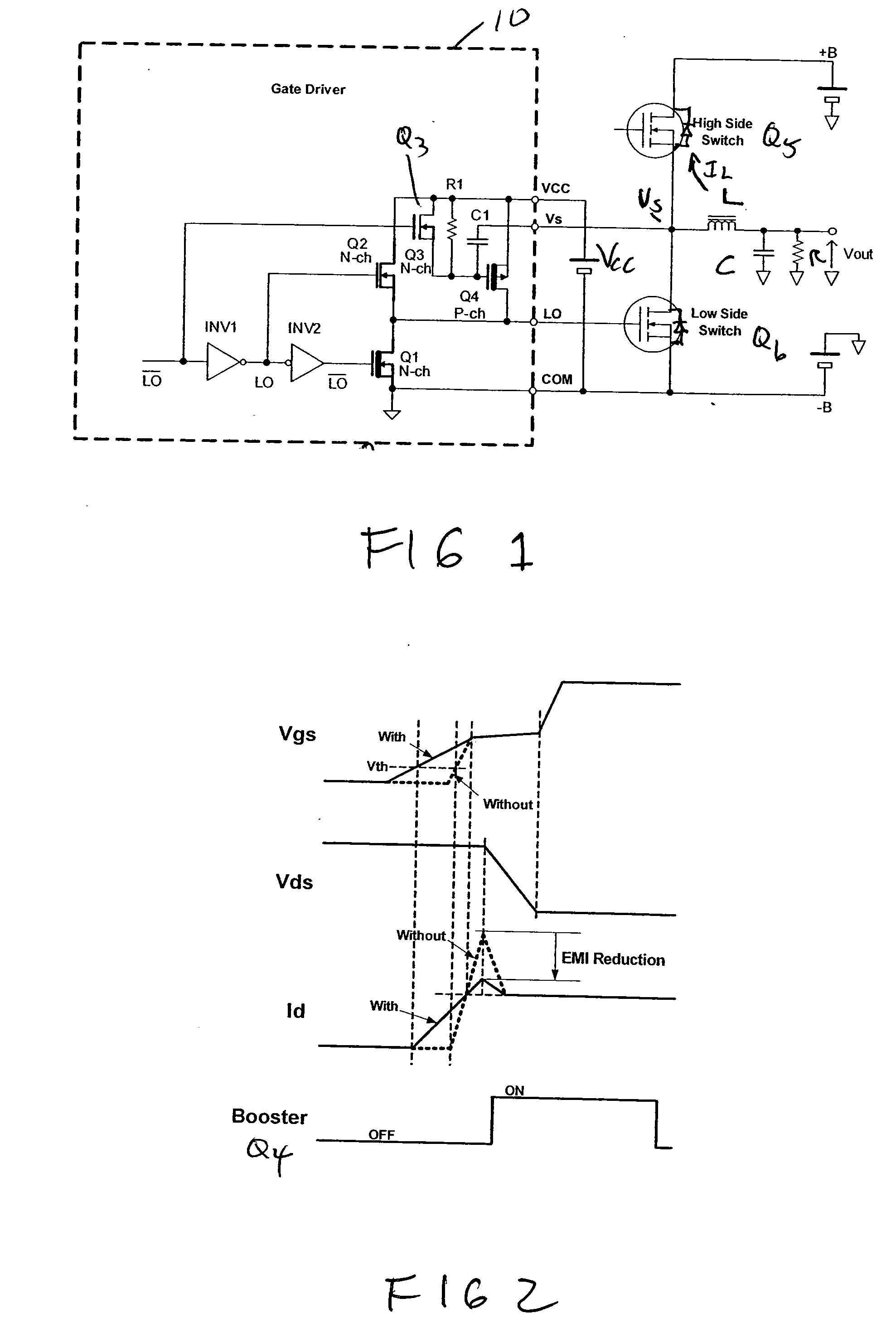
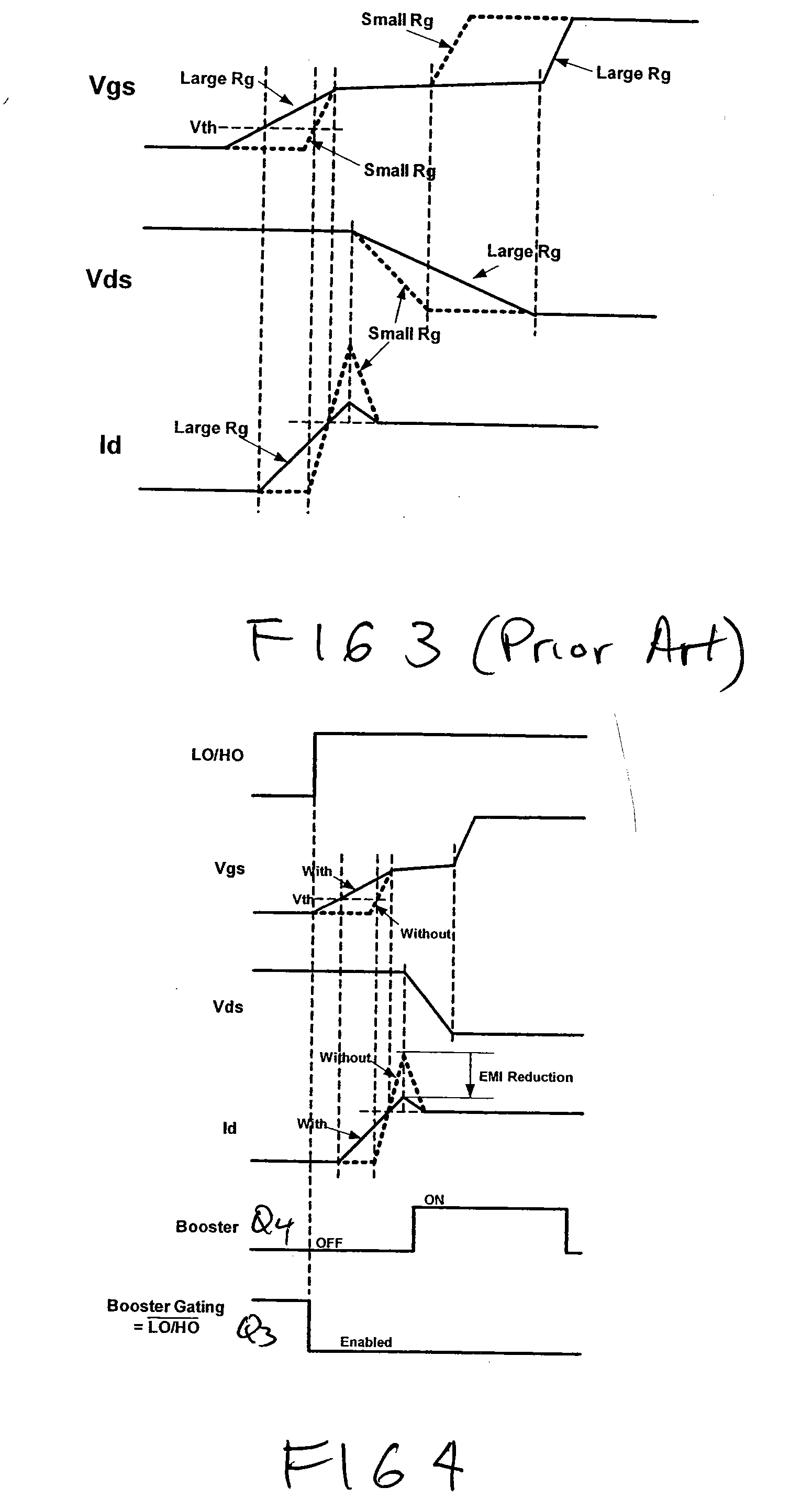
[0021] With reference to FIG. 1, the gate drive circuit of the invention comprises two current sourcing switches, e.g. FETs Q2 and Q4. Q2 is smaller than Q4 and sources less current. Transistor Q1 is driven in complementary fashion to Q2 by the inverter INV2. The common node between Q1 and Q2 drives the gate of the power MOSFET Q6, here shown as the low side switch, but the circuit is applicable to the high side power MOSFET Q5 also. Q5 and Q6 comprise a typical half bridge output stage, driving the load indicated as inductor L, capacitor C and resistor R across which VOUT is generated. The load may be, for example, a loudspeaker of a Class D audio amplifier.

[0022] A supply voltage VCC is provided to power the driver. A transistor Q3 acts as an enabling stage to allow the booster transistor Q4 to be turned on only when the LO signal is high, i.e., when LONOT is low. An RC circuit comprising a resistor R1 and capacitor C1 acts as a dv / dt detector.

[0023] Again turning to FIG. 1, ass...


PUM


Abstract

A gate drive circuit for driving the gate of a power transistor switch comprising a gate drive sourcing circuit supplying gate drive current to the power transistor switch, the gate drive sourcing circuit initially providing a first current to the gate of the power transistor switch and then providing a second current to the gate of the power transistor switch; a circuit for driving the gate drive sourcing circuit, the circuit having a first input for driving the gate drive sourcing circuit to turn on the power transistor switch by providing the first current, the circuit further having a second input coupled to a voltage across the power transistor switch and being controlled by the second input to cause the gate drive sourcing circuit to provide the second current when the voltage across the power transistor switch begins to drop as the power transistor switch begins to turn on.

Description

CROSS-REFERENCE TO RELATED APPLICATIONS [0001] This application claims the benefit and priority of U.S. Provisional patent application Ser. No. 60 / 736,799 filed Nov. 15, 2005 entitled GATE DRIVE FOR LOWER SWITCHING NOISE EMISSION, the entire disclosure of which is incorporated herein by reference.BACKGROUND OF THE INVENTION [0002] The invention relates to gate drive circuits and, in particular to such circuits with reduced electromagnetic interference (EMI) emission without sacrificing efficiency as compared to conventional circuits, such as those requiring large gate resistor insertion. [0003] In general, switching applications have a trade off between efficiency and EMI emissions. In order to get better efficiency, higher switching speed is required. The higher the speed, the steeper the transient which is generated due to stray inductances and capacitances and the greater the EMI. [0004] An aim of this invention is to reduce EMI emission without reducing efficiency significantly....

Claims


Application Information

Patent Timeline
Patent Type & Authority Applications(United States)
IPC IPC(8): H02H3/00
CPCH03K17/166H03K19/00361
Inventor HONDA, JUN
Owner INFINEON TECH AMERICAS CORP
Why Eureka
Try Eureka