CMOS compatible shallow-trench efuse structure and method

a shallow-trench, efuse technology, applied in the direction of semiconductor devices, semiconductor/solid-state device details, electrical apparatus, etc., can solve the problems of difficult to obtain a tight distribution of blow voltages derived from normal operating voltages, and the integration with standard complementary metal oxide semiconductor processing has been problematic, so as to achieve easy integration and minimize implementation costs

Inactive Publication Date: 2007-05-31
GOOGLE LLC
View PDF3 Cites 33 Cited by
  • Summary
  • Abstract
  • Description
  • Claims
  • Application Information

AI Technical Summary

Benefits of technology

[0005] In view of the state of prior art e-fuses mentioned above, there is a need to provide a semiconductor structure including at least one e-fuse and fabrication method which is easy to integrate with standard semiconductor technologies, thus minimizing implementation costs. Therefore, the present invention provides a semiconductor structure containing at least one e-fuse embedded within a fuse opening, e.g., trench, wherein the e-fuse is formed substantially at the same time as that of the trench isolation regions. More specifically, the e-fuse of the present invention is placed inside a fuse opening (e.g., trench) with its terminals connected to doped regions that are present in a semiconductor structure.

Problems solved by technology

Although e-fuses provide the above-mentioned benefits, integration with standard complementary metal oxide semiconductor (CMOS) processing has been problematic.
Furthermore, obtaining a tight distribution of blow voltages derived from normal operating voltages continues to be challenging.

Method used


Image

  • CMOS compatible shallow-trench efuse structure and method
  • CMOS compatible shallow-trench efuse structure and method
  • CMOS compatible shallow-trench efuse structure and method

Examples


second embodiment

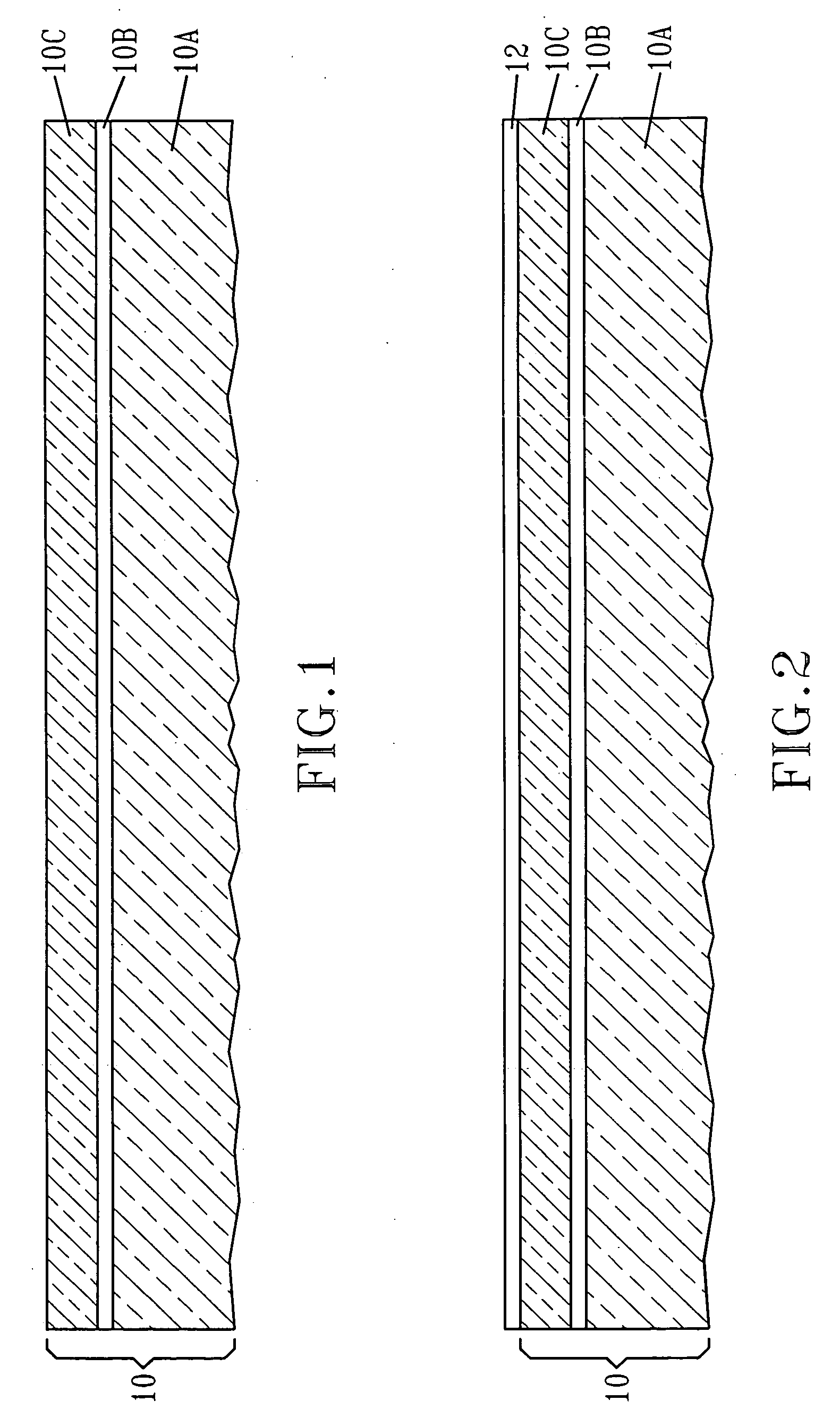
[0048] Reference is now made to FIGS. 12-16 which are pictorial representations illustrating the basic processing steps used in the present invention. Particularly, and in the embodiment shown in FIGS. 12-16 a bulk semiconductor substrate 50 is used. The bulk semiconductor substrate 50 comprises at least one of the semiconductor materials mentioned in above in connection with the SOI substrate 10. The bulk semiconductor substrate 50 may comprise a single crystal orientation or it may contain surface regions that have different crystal orientations. The latter substrates are hybrid substrates which can be formed utilizing techniques well known in the art. The bulk semiconductor substrate 50 can be doped, undoped or contain doped and undoped regions. Likewise, the bulk semiconductor substrate 50 can be strained, unstrained or contain regions of both strain and unstrain therein.

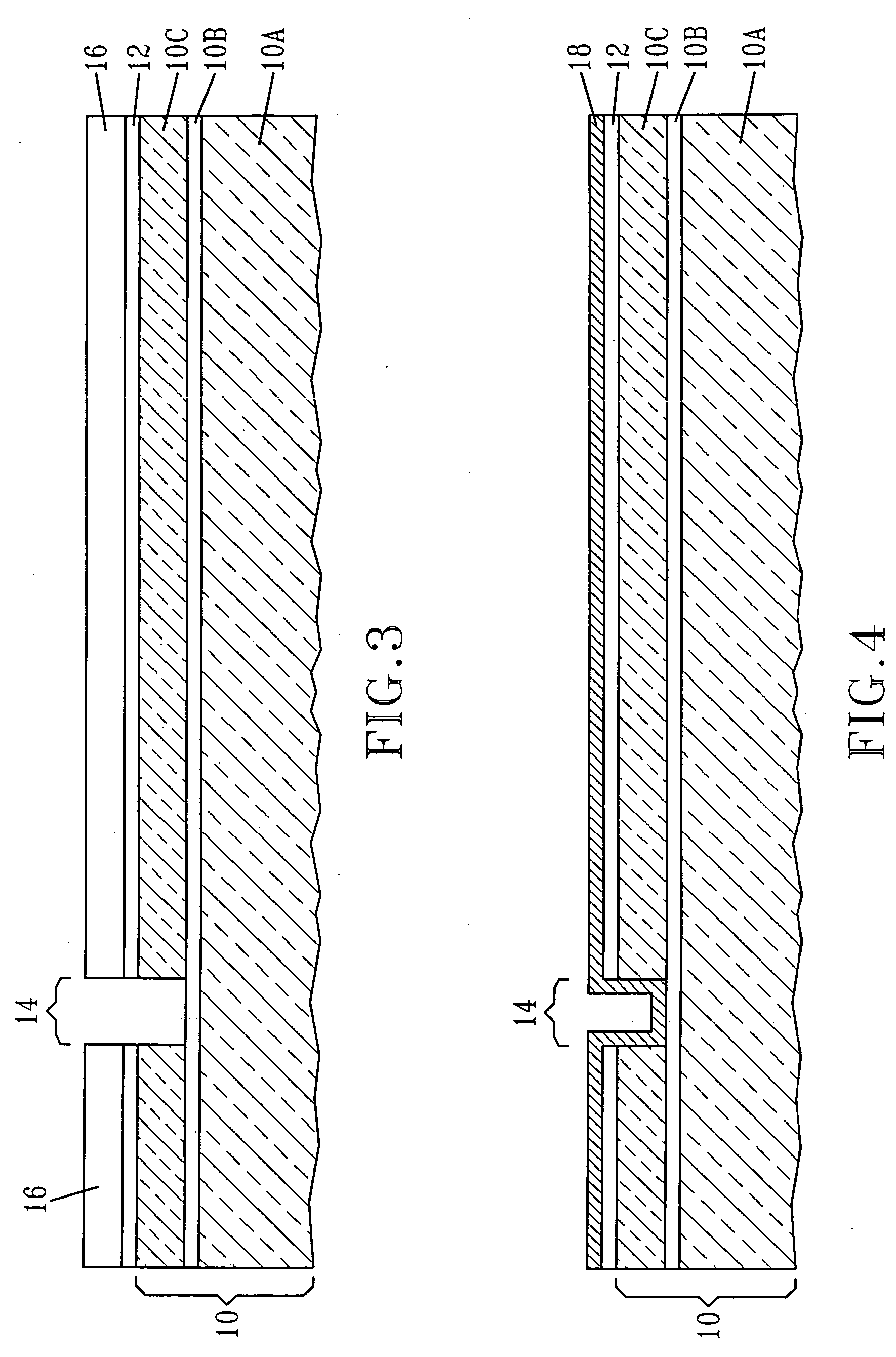
[0049]FIG. 12 shows the bulk semiconductor substrate 50 including a nitride or oxynitride dielectric cap 12 o...

first embodiment

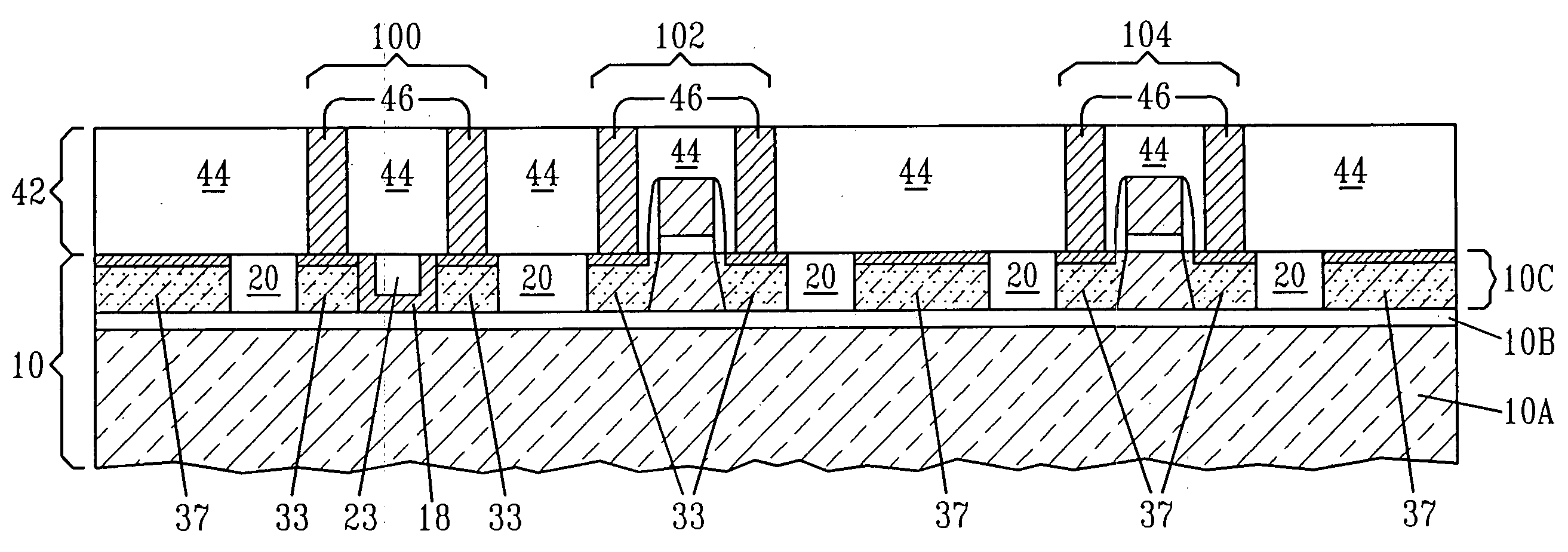
[0052] The remaining process steps as used in forming the fuse material 18 within the at least one opening 14 as described in the first embodiment above can now be employed. FIG. 16 depicts a portion of the bulk semiconductor substrate 50 that includes the e-fuse; note only the e-fuse location is shown in FIG. 16 and this drawing also does not show the presence of silicide region which are formed above each of the doped region. The latter omission was performed for clarity.

[0053] It is noted that the processing of the present invention, especially in regard to the first embodiment described above, provides an e-fuse material 18 inside the at least one opening 14 that presents a neck 110 at the bottom corners of the at least one opening 14. See, for example, FIG. 17. These necks result in current crowding during programming. When current pulse carries sufficient energy it can instantly generate a very high temperature in the vicinity of the neck regions and thus melt the fuse materia...


PUM


Abstract

A semiconductor structure including at least one e-fuse embedded within a trench that is located in a semiconductor substrate (bulk or semiconductor-on-insulator) is provided. In accordance with the present invention, the e-fuse is in electrical contact with a dopant region that is located within the semiconductor substrate. The present invention also provides a method of fabricating such a semiconductor structure in which the embedded e-fuse is formed substantially at the same time with the trench isolation regions.

Description

FIELD OF THE INVENTION [0001] The present invention relates to a semiconductor structure and a method of fabricating the same. More particularly, the present invention provides a semiconductor structure including at least one e-fuse embedded within a fuse opening (e.g., trench) that is located in a semiconductor substrate. In accordance with the present invention, the e-fuse is in electrical contact with a dopant region that is also present within the semiconductor substrate. The present invention also provides a method of fabricating such a semiconductor structure. BACKGROUND OF THE INVENTION [0002] Current semiconductors and other similar devices are often manufactured with a large number of fuse elements which are used to invoke the replacement of failing cells or components, and provide direct alternative current (DAC) trimming, etc. During testing of the device, selected fuses are usually blown by either a laser beam or an electrical current, depending on the design of the fuse...

Claims


Application Information

Patent Timeline
Patent Type & Authority Applications(United States)
IPC IPC(8): H01L29/00
CPCH01L21/268H01L21/84H01L23/5256H01L27/1203H01L2924/0002H01L2924/00
Inventor HSU, LOUISMANDELMAN, JACKTONTI, WILLIAMYANG, CHIH-CHAO
Owner GOOGLE LLC
Why Eureka
Try Eureka