

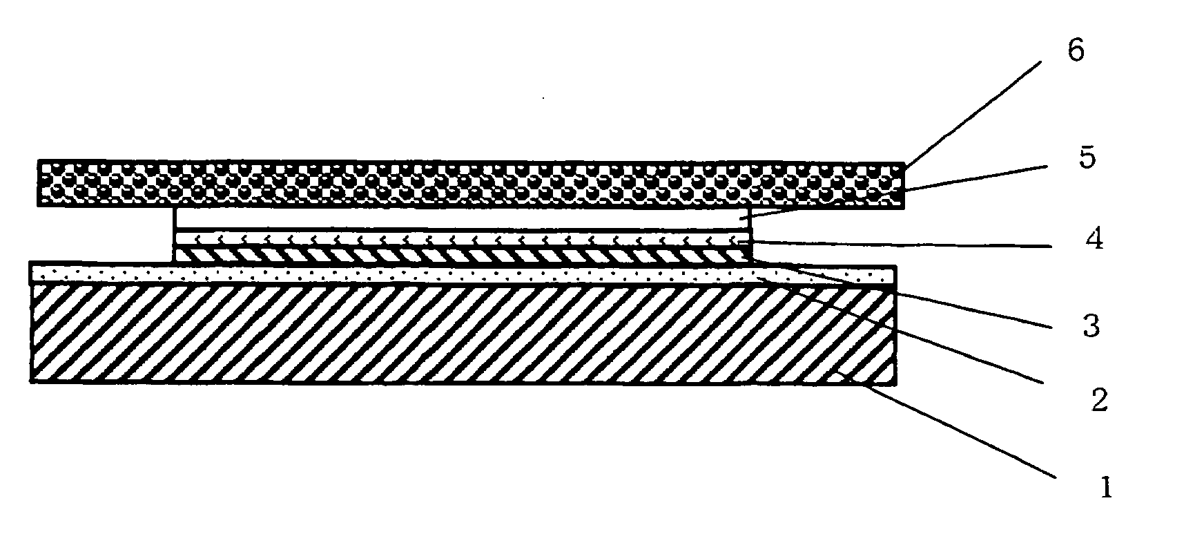
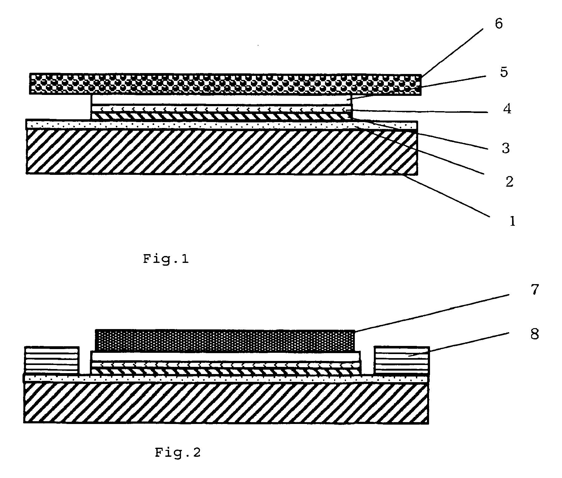
Dicing and die bonding adhesive tape
- Summary
- Abstract
- Description
- Claims
- Application Information
AI Technical Summary
Benefits of technology
Problems solved by technology
Method used
Image

Examples
preparation example 1
[0094] A pressure sensitive adhesive silicone composition-I was prepared from 108.3 parts by weight of a 60 wt % toluene solution of methylpolysiloxane resin composed of (CH3)3SiO1 / 2 units and Sio2 units in a molar ratio of 1.1:1; 35 parts by weight of a raw rubber-like dimethylpolysiloxane having a polymerization degree of 2,000, and vinyl groups at terminal and in side chains in an amount of 0.002 mole per 100 g of the dimethylpolysiloxane; and 142.4 parts by weight of toluene, 0.32 parts by weight of an organopolysiloxane compound having hydrogen atoms bonded to silicon atoms represented by the following structure; a solution of chloroplatinic acid modified with 2-ethylhexanol in an amount of 40 ppm as platinum metal; and 0.15 parts by weight of 3-methyl-1-butyn-3-ol as a reaction retarder.
preparation example 2
[0095] A pressure sensitive adhesive silicone composition-II was prepared in the same manner as in Preparation Example 1 from 75 parts by weight of a 60 wt % toluene solution of methylpolysiloxane resin composed of (CH3)3Sio1 / 2 units and SiO2 units in a molar ratio of 1.1:1; 55 parts by weight of a raw rubber-like dimethylpolysiloxane having a polymerization degree of 2,000, and vinyl groups at terminal and in side chains in an amount of 0.002 mole per 100 g of the dimethylpolysiloxane; and 155.7 parts by weight of toluene, 0.51 parts by weight of an organopolysiloxane compound having hydrogen atoms bonded to silicon atoms represented by the above structure; a solution of chloroplatinic acid modified with 2-ethylhexanol in such an amount that platinum content is 40 ppm; and 0.15 parts by weight of 3-methyl-1-butyn-3-ol as a reaction retarder.
Preparation of Pressure Sensitive Adhesive Silicone Composition for PSA Layer (B)
preparation example 3
[0096] A pressure sensitive adhesive silicone composition-III was prepared from 33.33 parts by weight of a 60 wt % toluene solution of methylpolysiloxane resin composed of (CH3)3SiO1 / 2 units and SiO2 units in a molar ratio of 1.1:1; 80 parts by weight of a raw rubber-like dimethylpolysiloxane having a polymerization degree of 2,000, and vinyl groups at terminal and in side chains in an amount of 0.002 mole per 100 g of the dimethylpolysiloxane; and 172 parts by weight of toluene were solved to obtain a homogeneous mixture. To this mixture were added 0.68 parts by weight of an organopolysiloxane compound having hydrogen atoms bonded to silicon atoms represented by the following structure and 0.24 parts by weight of 3-methyl-1-butyn-3-ol as a reaction retarder. Then a solution of chloroplatinic acid modified with 2-ethylhexanol was added in such an amount that platinum content is 40 ppm.
PUM
| Property | Measurement | Unit |
|---|---|---|
| Thickness | aaaaa | aaaaa |
| Energy | aaaaa | aaaaa |
| Energy | aaaaa | aaaaa |
Abstract
Description
Claims
Application Information