Semiconductor device and operating method thereof

a technology of semiconductor devices and memory cells, applied in semiconductor devices, digital storage, instruments, etc., can solve the problems of increasing manufacturing costs, greatly affecting the integration degree of wires, etc., and achieves the effects of saving space, reducing manufacturing costs, and reliable outpu

Inactive Publication Date: 2007-05-31
SEMICON ENERGY LAB CO LTD
View PDF12 Cites 5 Cited by
  • Summary
  • Abstract
  • Description
  • Claims
  • Application Information

AI Technical Summary

Benefits of technology

[0024] A word line and a data line are controlled with a reset signal, so that data can be reliably outputted.
[0025] In addition, a memory cell is constituted of one transistor which is connected to a word line, a data line, and a GND line, and space can be saved. By using the memory cell in which space can be saved, the number of memory cells in a substrate can be large and cost can be reduced.
[0026] In the memory cell, the transistor is not connected to GND, and rewriting of data can be easily done by modifying either a contact mask or a wire mask for rewriting data.

Problems solved by technology

Such wires greatly affect the integration degree of the ROM.
In the case of modifying data, a mask for exposure which is used for forming a wire is required to be modified, thereby increasing manufacturing cost.

Method used


Image

  • Semiconductor device and operating method thereof
  • Semiconductor device and operating method thereof
  • Semiconductor device and operating method thereof

Examples


embodiment mode 1

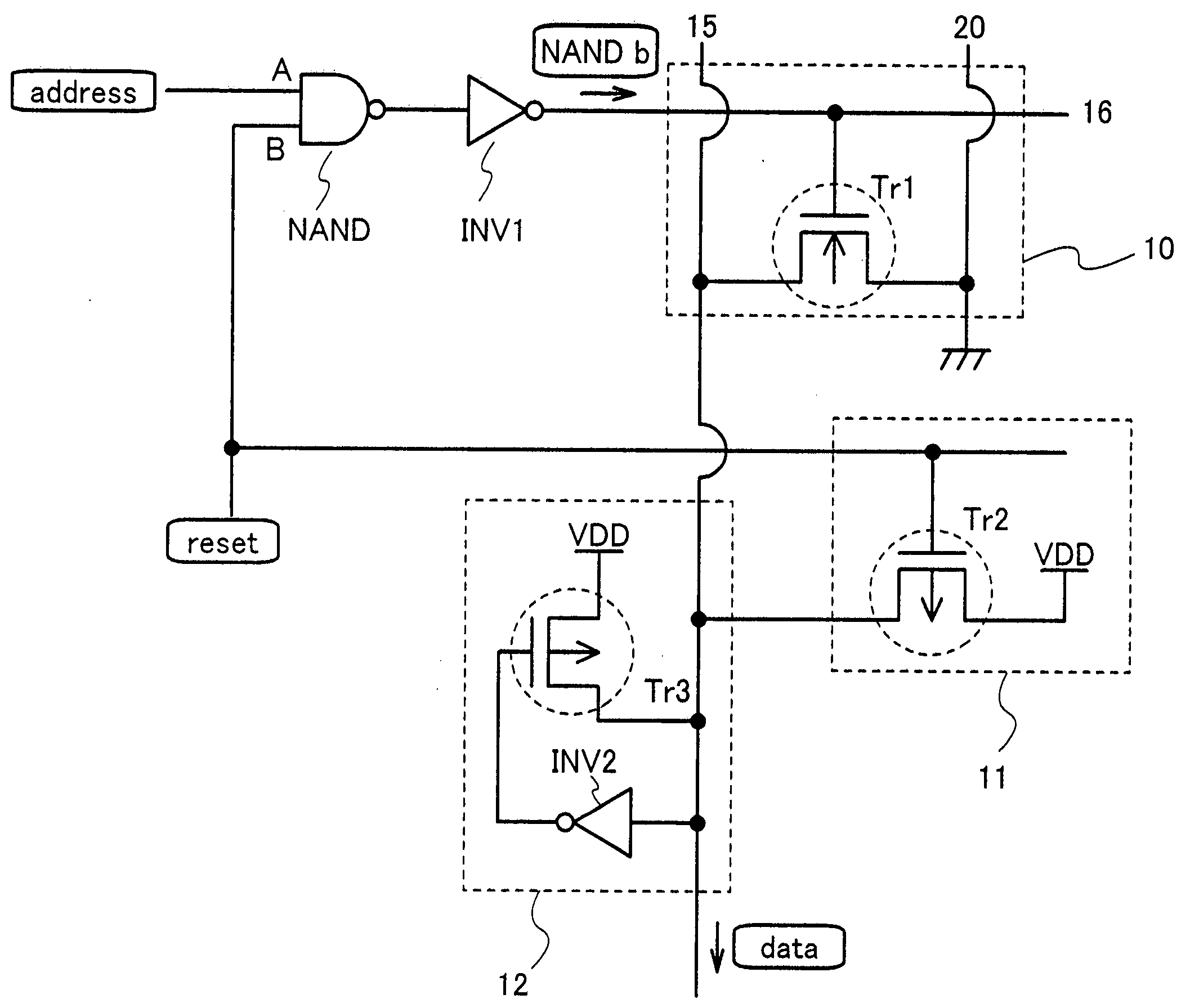
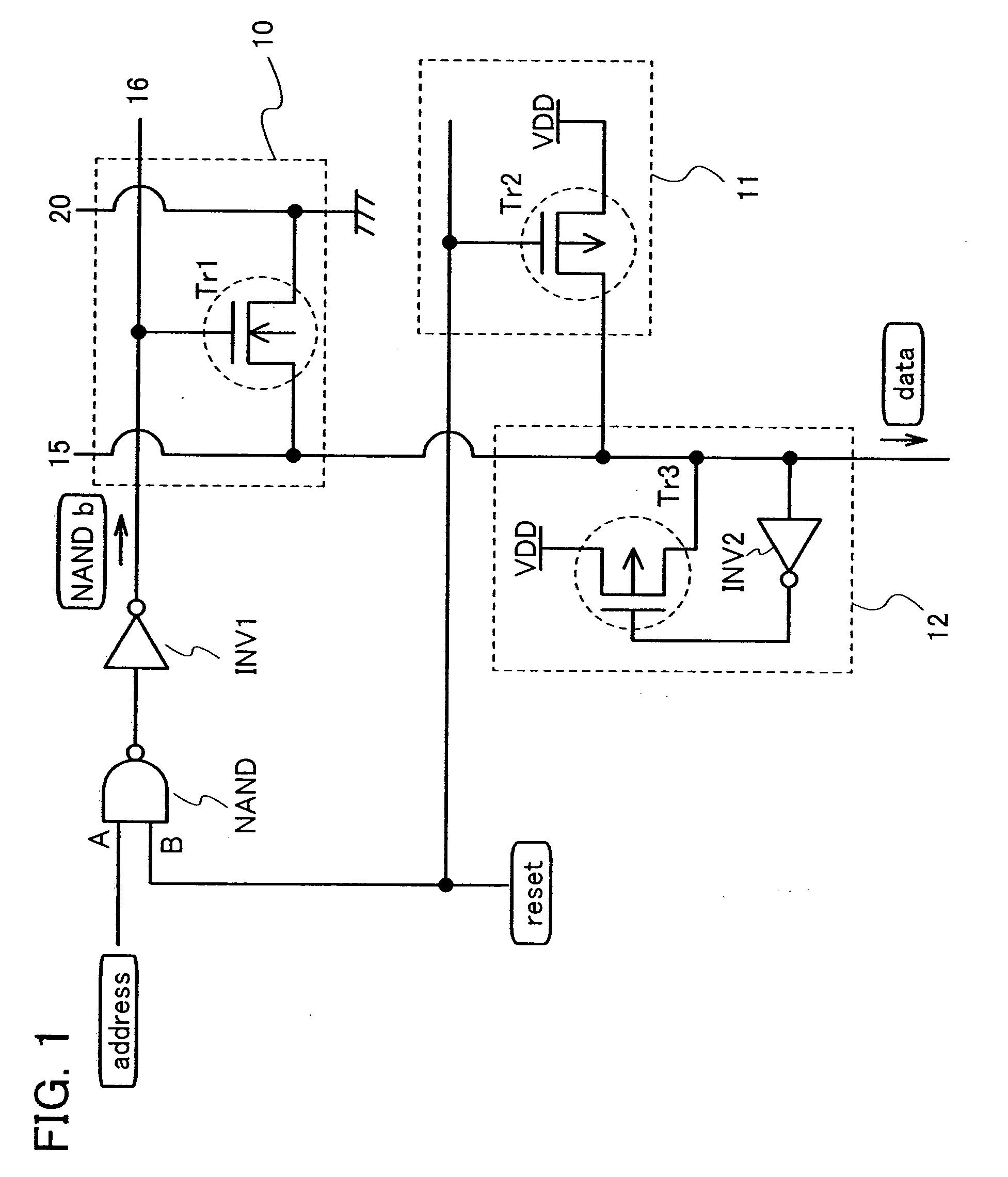
[0039] A structure of a semiconductor device having a memory cell and the like and an operation thereof are described in this embodiment mode.

[0040]FIG. 1 shows a memory cell 10, and a precharge circuit 11 and a sense amplifier circuit 12 which are connected to the memory cell 10 through a data line 15. The memory cell 10 includes an N-channel transistor (Tr1), and a gate terminal of the transistor (Tr1) is connected to a word line 16. An inverter (INV1) and a NAND are connected to the word line 16 in series, and an address signal (address) and a reset signal (reset) are inputted to input terminals of the NAND. A signal based on the address signal and the reset signal is outputted from an output terminal of the NAND, and this signal is inverted by the INV1. This signal which has been inverted, that is an inverted signal is inputted to the gate terminal of the transistor (Tr1). The present invention is not limited to the combination of the NAND and the INV1 as long as the signal bas...

embodiment mode 2

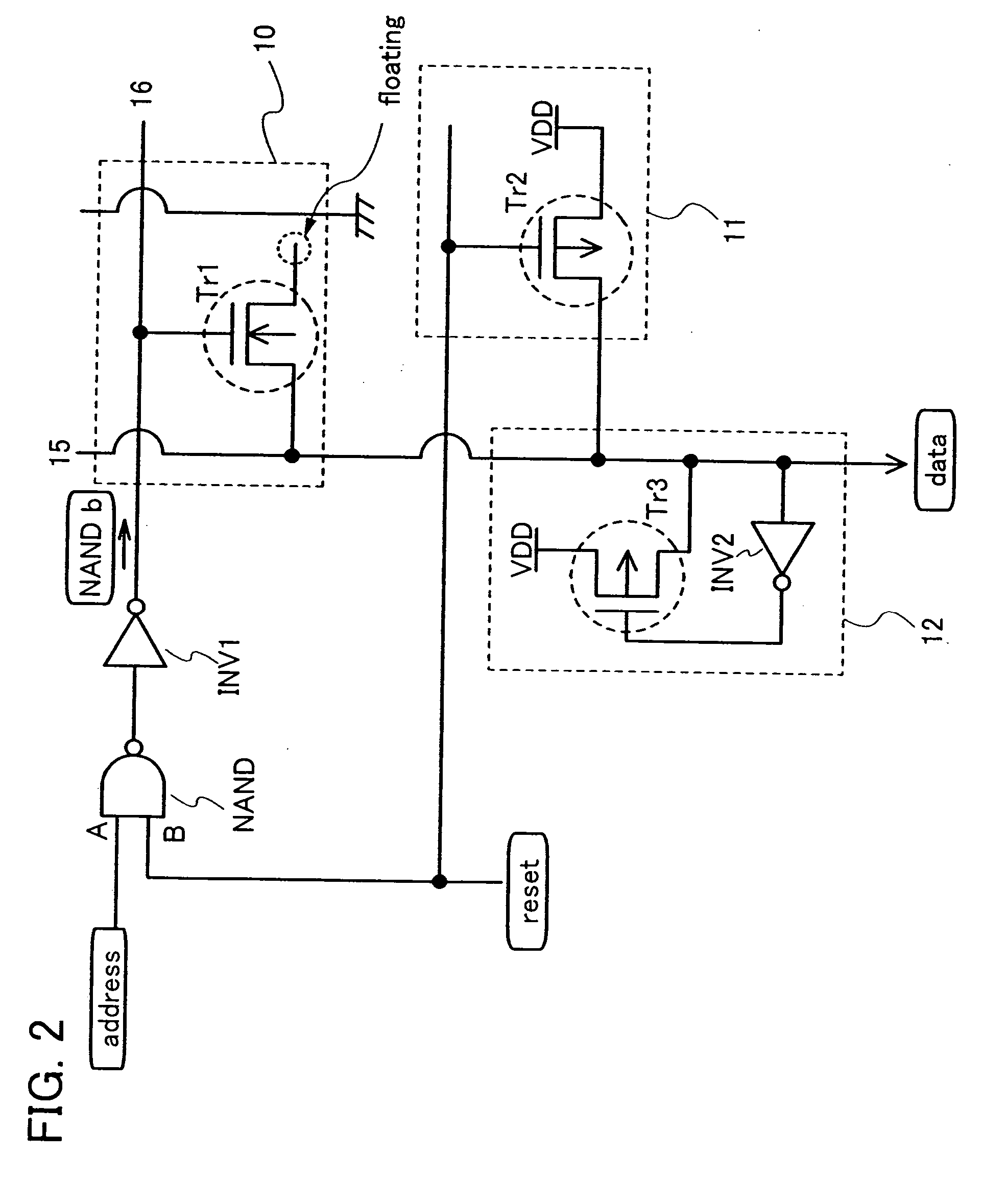
[0051] A structure of a semiconductor device having a memory cell which is different from the aforementioned embodiment mode, or the like, and an operation of the semiconductor device are described in this embodiment mode.

[0052]FIG. 2 shows the memory cell 10, the precharge circuit 11 and the sense amplifier circuit 12 which are connected to the memory cell 10 through the data line 15. A structural difference between FIG. 1 and FIG. 2 is in that the transistor (Tr1) of the memory cell 10 is not connected to GND and in a floating state. The transistor (Tr1) in the memory cell is not connected in this manner; therefore, data can be changed by modifying either a contact mask or a wire mask at the time of rewriting data of the memory cell. Through a simple process in this manner, the data of the memory cell can be rewritten. Since the other configuration is similar, description is omitted.

[0053]FIG. 4 shows a timing chart. A series of operations which is divided into a period 5, a per...

embodiment mode 3

[0061] In this embodiment mode, as a structural example of a semiconductor device of the present invention, a wireless chip provided with a semiconductor device having a memory cell is described. A method for manufacturing the wireless chip is described below.

[0062] In FIG. 5A, a release layer 601, an insulating layer 602, and a semiconductor film 603 are sequentially formed over a substrate having an insulating surface (hereinafter referred to as an insulating substrate) 600. As the insulating substrate 600, a glass substrate, a quartz substrate, a substrate which is made of silicon, a metal substrate, a plastic substrate, or the like can be employed. In addition, the insulating substrate 600 may be thinned by polishing. By employing the thinned insulating substrate, a finished product can be reduced in weight and thickness.

[0063] The release layer 601 can be formed of an element selected from W, Ti, Ta, Mo, Nb, Nd, Ni, Co, Zr, Zn, Ru, Rh, Pd, Os, Ir, or Si, an alloy material con...


PUM


Abstract

An object is to provide a semiconductor device capable of reducing an area of the semiconductor device, reading data reliably, and simplifying replacement of data. A memory cell and a data line are controlled with a reset signal, so that data can be reliably outputted in the semiconductor device. In addition, an element of data holding unit is included, and the data holding unit includes a plurality of memory cells. The area can be reduced by using such a memory cell. A transistor is not connected to GND, thereby simplifying the replacement of data in the memory cell.

Description

TECHNICAL FIELD [0001] The present invention relates to a semiconductor device having a memory area and a method for operating the device. BACKGROUND ART [0002] With development of computer technologies, a large-capacity memory has been required. To enlarge a capacity of a memory, the number of memory cells may be increased. However, when the number of memory cells is increased, the area is increased, and downsizing of a memory and a computer having the memory is limited. [0003] Such a memory includes a RAM (Random Access Memory) or a ROM (Read Only Memory). The RAM is a rewritable memory, and the ROM is a memory which is readable only. [0004] The RAM and the ROM each have a word line and a data line, and a memory cell is formed at the intersection of these lines. Predetermined information can be made by using binary states (0 and 1) of the memory cell. [0005] As for the ROM, in order to reduce the number of revised masks and improve degree of integration, a structure of a multivalu...

Claims


Application Information

Patent Timeline
Patent Type & Authority Applications(United States)
IPC IPC(8): G11C7/00
CPCG11C17/12H01L27/105H01L27/112H01L27/13H01L27/1214H01L27/1266H01L27/11293H10B20/65H10B20/00
Inventor OHSHIMA, KAZUAKI
Owner SEMICON ENERGY LAB CO LTD
Why Eureka
Try Eureka