

Method for production of semiconductor device
- Summary
- Abstract
- Description
- Claims
- Application Information
AI Technical Summary
Benefits of technology
Problems solved by technology
Method used
Image

Examples
Embodiment Construction
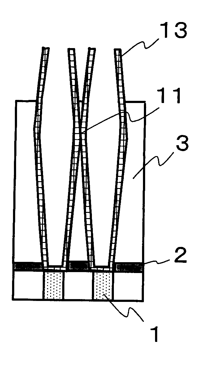
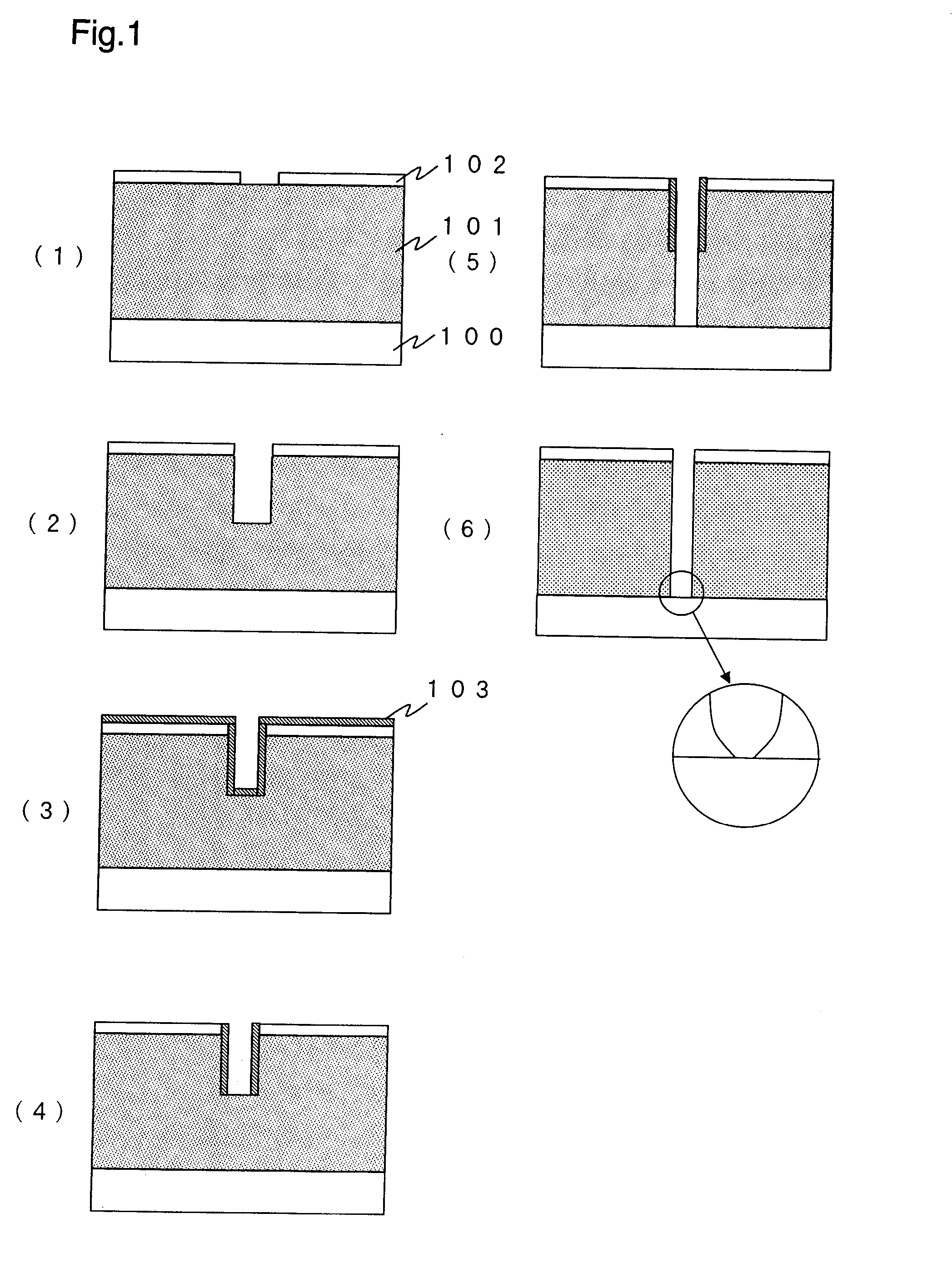
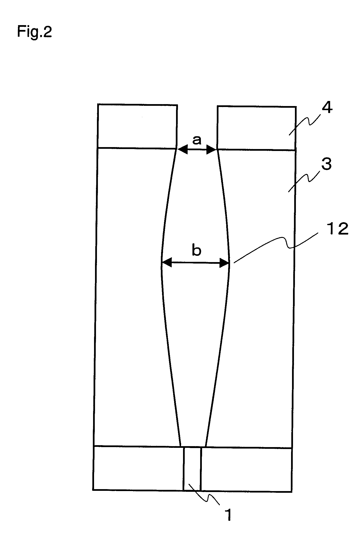
[0044] (Method for Production of Semiconductor Device)
[0045] The present invention provides a method for production of a semiconductor device having on a substrate the first insulating film, the second insulating film and the third insulating film in this order and having a hole extending through the first insulating film, the second insulating film and the third insulating film. The production method comprises the steps of:
[0046] (1) depositing on the substrate the first insulating film, the second insulating film and the third insulating film in this order;
[0047] (2) forming a first hole extending through the third insulating film along a direction of the thickness thereof;
[0048] (3) forming a second hole in the second insulating film in the lower part of the first hole to a depth at which a bowing shape does not occur by anisotropic etching using the third insulating film as a mask;
[0049] (4) forming a fourth film on the side surfaces of the first and the second holes;
[0050...
PUM
 Abstract
Description
Claims
Application Information