Semiconductor device

a technology of semiconductors and oscillation signals, applied in the direction of semiconductor devices, electrical equipment, transmission, etc., can solve the problems of not always being able to stably generate highly accurate reference oscillation signals, and inability to realize high-frequency frequency, etc., to achieve convenient mounting of components, reduce system size, and high density packing

Inactive Publication Date: 2007-06-07
RENESAS TECH CORP
View PDF1 Cites 8 Cited by
  • Summary
  • Abstract
  • Description
  • Claims
  • Application Information

AI Technical Summary

Benefits of technology

[0019] A mobile phone system, for example, in which high density packing of components may be advanced by comprising the varactor diode on the semiconductor chip as explained above can realize reduction in size of system, easier mounting of components and reduction in component inspection cost. Moreover, formation of a plurality of built-in varactor diodes can also realize highly accurate adjustment of the reference frequency.
[0020] Moreover, the semiconductor device of the present invention is characterized in that a first semiconductor region of a first conductivity type connected to the frequency adjustment node is formed to the varactor diode of the semiconductor layer explained above and a second semiconductor region of a second conductivity type opposing to the first conductivity type is formed between the first insulating layer explained above and the first semiconductor region. According to the structure explained above, even when noise is generated toward the varactor diode via the supporting substrate and the first insulating layer, for example, from the second circuit and frequency converting circuit or the like explained above, the reference frequency can be stabilized, because such noise is alleviated in the second semiconductor region until the noise is transferred to the frequency adjustment node.

Problems solved by technology

However, if the crystal-controlled vibrator has fluctuation or the like in manufacturing process, such highly accurate frequency cannot be realized.
However, the inventors of the present invention have proved through investigation that it is not always possible to stably generate highly accurate frequency of the reference oscillation signal depending on a structure of the front-end IC explained above.

Method used


Image

  • Semiconductor device
  • Semiconductor device
  • Semiconductor device

Examples


first embodiment

[0040] A semiconductor device shown in the first embodiment of the present invention is characterized, for example, in a front-end circuit and is mainly characterized, although explained later in detail, in a structure of a varactor diode included in such front-end circuit.

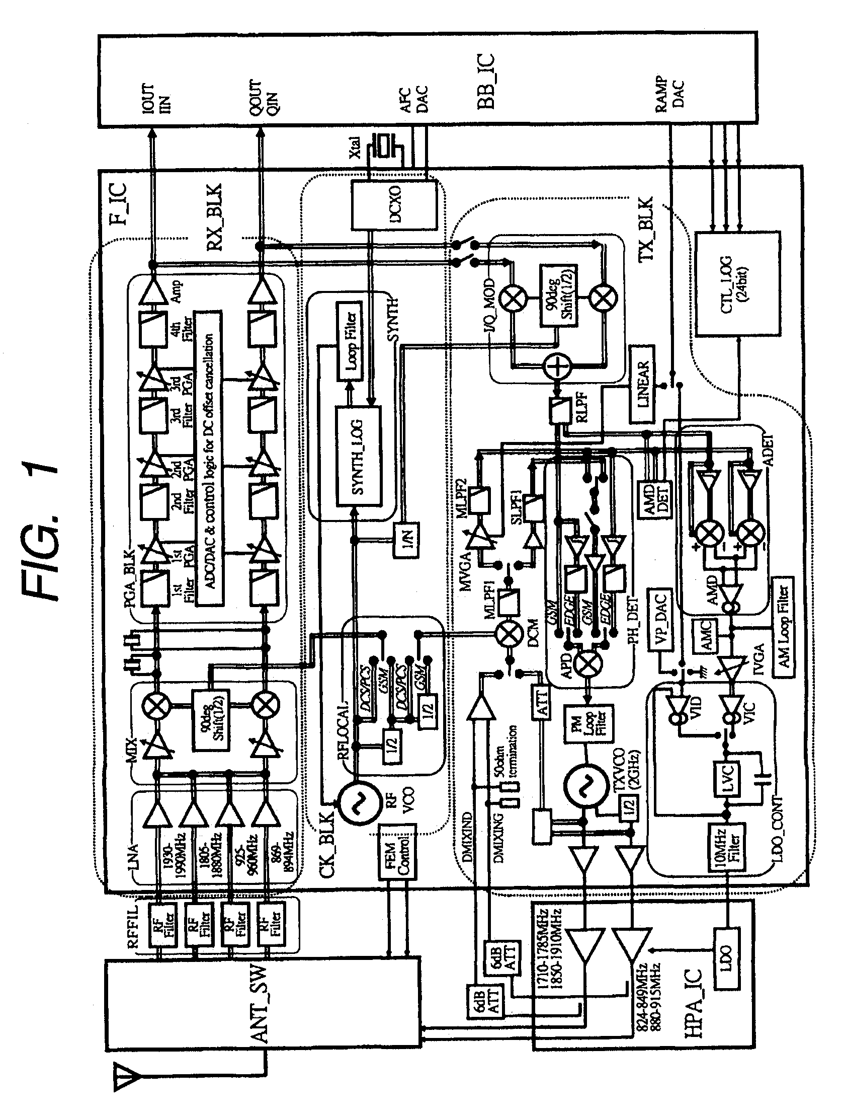
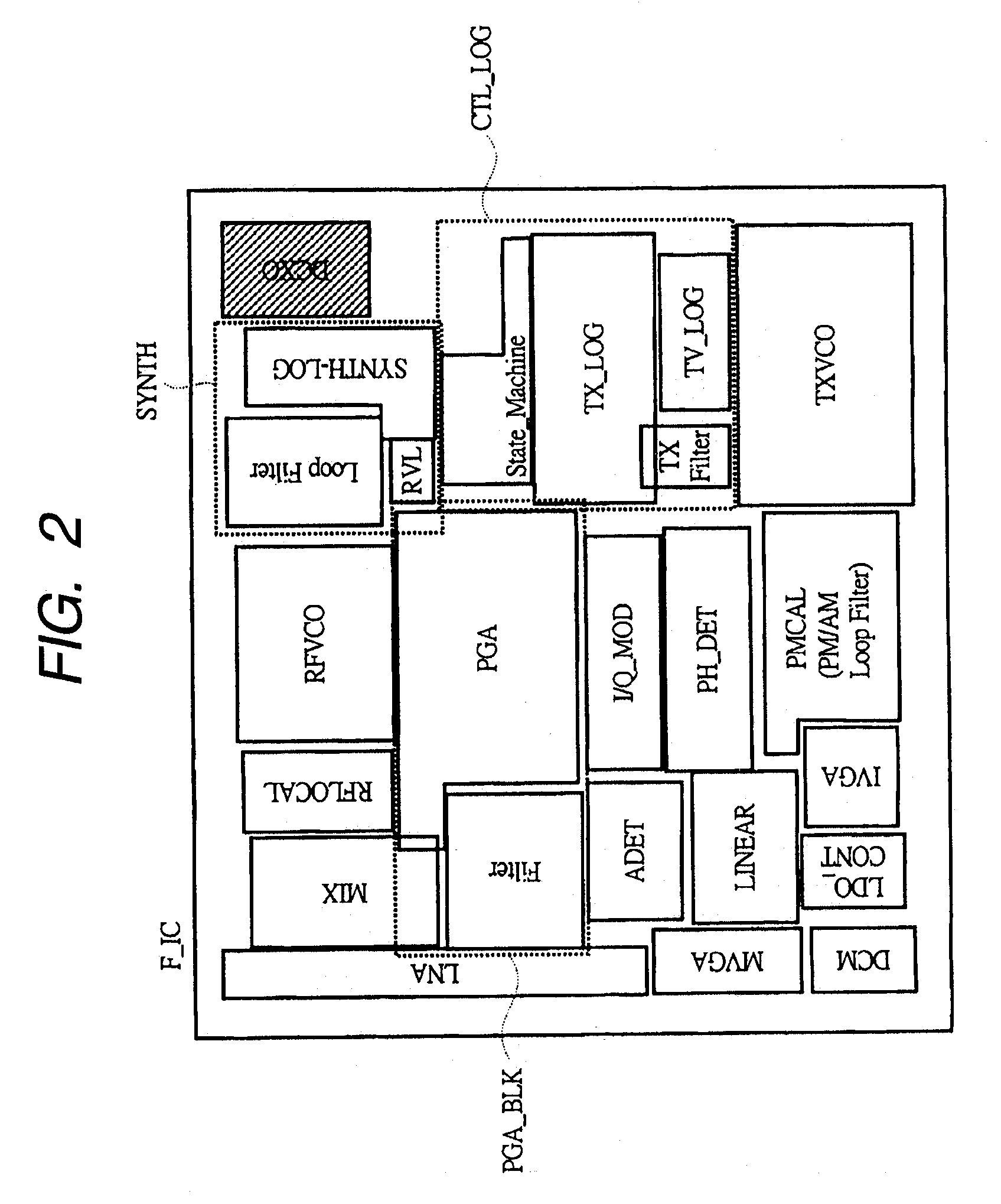
[0041]FIG. 1 is a block diagram showing an example of structure of a radio communication system to which a semiconductor device of the first embodiment of the present invention is applied. The radio communication system of FIG. 1 is constituted of a switch ANT_SW for switching connection of antenna ANT in accordance with transmission and reception, a radio-frequency filter RFFIL for removing unwanted wave from the receiving signal, a high frequency power amplifier HPA_IC for amplifying the transmitting signal, an front-end circuit F_IC for demodulating the receiving signal and modulating the transmitting signal, and a baseband circuit BB_IC. Here, the front-end circuit (semiconductor device) F_IC is formed in one...

second embodiment

[0068] A semiconductor device disclosed in the second embodiment is formed through modification of the structure of the varactor diode shown in FIG. 5B.

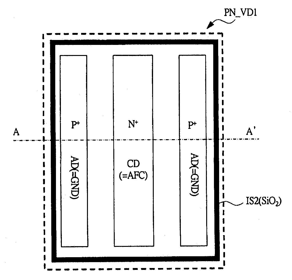
[0069]FIGS. 7A and 7B are a diagrams showing a modification example of the varactor diode of FIG. 5B in the semiconductor device of the second embodiment of the present invention. FIG. 7A is a cross-sectional view and FIG. 7B is a graph showing evaluation result. The varactor diode PN_VD2 of FIG. 7A is different from the varactor diode PN_VD1 of FIG. 5B in the arrangement of the anode node AD and cathode node CD and conductivity type of each semiconductor region corresponding to such arrangement. Only difference from the structure of FIG. 5B will be explained below.

[0070] In the varactor diode PN_VD2 of FIG. 7A, the p++ type semiconductor region (P++), and n type semiconductor region (N) are sequentially formed toward the main surface of the semiconductor layer DF from the embedded insulating layer IS1. In the n type semiconductor ...

third embodiment

[0072] The semiconductor device disclosed in the third embodiment is formed through modification of the varactor diode shown in FIG. 5B like the second embodiment.

[0073]FIGS. 8A and 8B are diagrams showing another embodiment of the varactor diode of FIG. 5B in the semiconductor device of the third embodiment of the present invention. FIG. 8A is a cross-sectional view and FIG. 8B is a graph showing the evaluation result. The varactor diode PN_VD3 of FIG. 8A is identical in the arrangement and structure of the anode node AD and cathode node CD in comparison with the varactor diode PN_VD1 of FIG. 5B. Difference from the structure of FIG. 5B is only that the n−type semiconductor region (N−) on the embedded insulating layer IS1 in FIG. 5B is changed to the p++ type semiconductor region (P++) in FIG. 8A.

[0074] In the structure explained above, noise transferred via the embedded insulating layer IS1 from the semiconductor substrate SUB is further transferred to the n+ type semiconductor ...


PUM


Abstract

The semiconductor device provided assures stable communication processes. For example, a varactor diode for adjusting the reference frequency is comprised within a digital crystal-controlled oscillating circuit provided as an internal circuit of the front-end circuit for generating the reference oscillation signal of a PLL circuit or the like. The varactor diode is formed to a semiconductor layer DF of the so-called SOI structure in the structure where an embedded insulating layer, a ntype semiconductor region, a p type semiconductor region, and a n+ type semiconductor region are formed in this sequence and the n+ type semiconductor region is connected to a cathode node which becomes the frequency adjusting node. Moreover, a p+ type semiconductor region connected to the p type semiconductor region is formed in both sides of the n+ type semiconductor region, and this p+ type semiconductor region is connected to an anode node to which the ground voltage is applied. Accordingly, noise transferred to a frequency adjusting node via the embedded insulating layer from a semiconductor substrate can be reduced.

Description

CROSS-REFERENCE TO RELATED APPLICATION [0001] The present application claims priority from Japanese patent application No. 2005-351846 filed on Dec. 6, 2005, the content of which is hereby incorporated by reference into this application. BACKGROUND OF THE INVENTION [0002] The present invention relates to a semiconductor device and particularly to a technology which may be applied effectively to a semiconductor device used to a mobile phone system to conduct up-conversion and down-conversion. [0003] For example, the patent document 1 discloses the technology to individually provide the ground of each circuit in a structure where a semiconductor chip including a plurality of circuits is mounted to a package such as QFN (Quad Flat Non-leaded package) corresponding to down-bonding. In more concrete, the patent document 1 explained above discloses a structure that a ground pad of a low-noise amplifier belonging to the receiving system is bonded in direct to an external lead for a semicon...

Claims


Application Information

Patent Timeline
Patent Type & Authority Applications(United States)
IPC IPC(8): H01L29/93
CPCH01L24/32H01L27/1203H01L2924/1305H01L2924/01033H01L2924/01023H01L2924/01006H01L2924/01005H04B1/40H01L2924/3025H01L2924/15311H01L2924/01082H01L2924/01061H01L2924/01051H01L2924/01047H01L2224/73265H01L2224/48227H01L2224/48091H01L2224/32225H01L2224/32014H01L29/93H01L2924/00014H01L2924/00H01L2924/00012H01L24/73H01L2924/12034H01L2924/12036H01L2924/14H01L2924/181
Inventor SUZUKI, KENTAROONO, IKUYADANNO, TADATOSHI
Owner RENESAS TECH CORP
Why Eureka
Try Eureka