Integrated Circuit Micro-Cooler Having Tubes of a CNT Array in Essentially the Same Height over a Surface

a technology of integrated circuits and cooling tubes, which is applied in the direction of electrical equipment, semiconductor devices, and semiconductor/solid-state device details, etc., can solve the problems of increasing the total die-to-heat sink resistance, increasing the difficulty of heat transfer, and unable to dissipate the heat generated by current ics

Inactive Publication Date: 2007-06-07
NANOCONDUCTION
View PDF34 Cites 52 Cited by
  • Summary
  • Abstract
  • Description
  • Claims
  • Application Information

AI Technical Summary

Problems solved by technology

Prior art techniques that are used to cool semiconductor ICs incorporate the use of large and expensive chip packaging having externally mounted, finned heat sinks coupled to the ceramic or plastic encapsulated IC chip.
In the video processing and CPU application areas, the ability to dissipate the heat being generated by current ICs is becoming a serious limitation in the advance of technology.
These multiple interfaces have the undesired side effect of increasing total die-to-heat sink resistance and making heat transfer more difficult.
These materials, while better than solid surface / surface contact, still have a relatively poor thermal conductivity when compared to solid metals.
As a result, the backside chip surface interface still presents a significant thermal resistance, which limits the power that can be extracted from the chip.
However, the polymeric filler does little to spread heat laterally, potentially creating localized hot spots on the device surface.
The use of bundles of aligned carbon nano-tubes may result in reduced thermal conduction as well.
The '471 disclosure, however, fails to provide any method to reduce matting and nano-tube to nano-tube contact, which reduces the effective thermal conductivity of the structure.
Although CVD diamond films are good conductors, they may not be thermally compatible, from an expansion perspective, with a number of other metallic materials used in various heat sink structures.
Additionally, commonly known techniques for growing carbon nano-tubes preclude carbon nanotube deposition directly on a silicon circuit die because these techniques require temperatures in the range of 700 to 800° C. Exposing a completed circuit die to these elevated temperatures is not a recommended practice.

Method used


Image

  • Integrated Circuit Micro-Cooler Having Tubes of a CNT Array in Essentially the Same Height over a Surface
  • Integrated Circuit Micro-Cooler Having Tubes of a CNT Array in Essentially the Same Height over a Surface
  • Integrated Circuit Micro-Cooler Having Tubes of a CNT Array in Essentially the Same Height over a Surface

Examples


Embodiment Construction

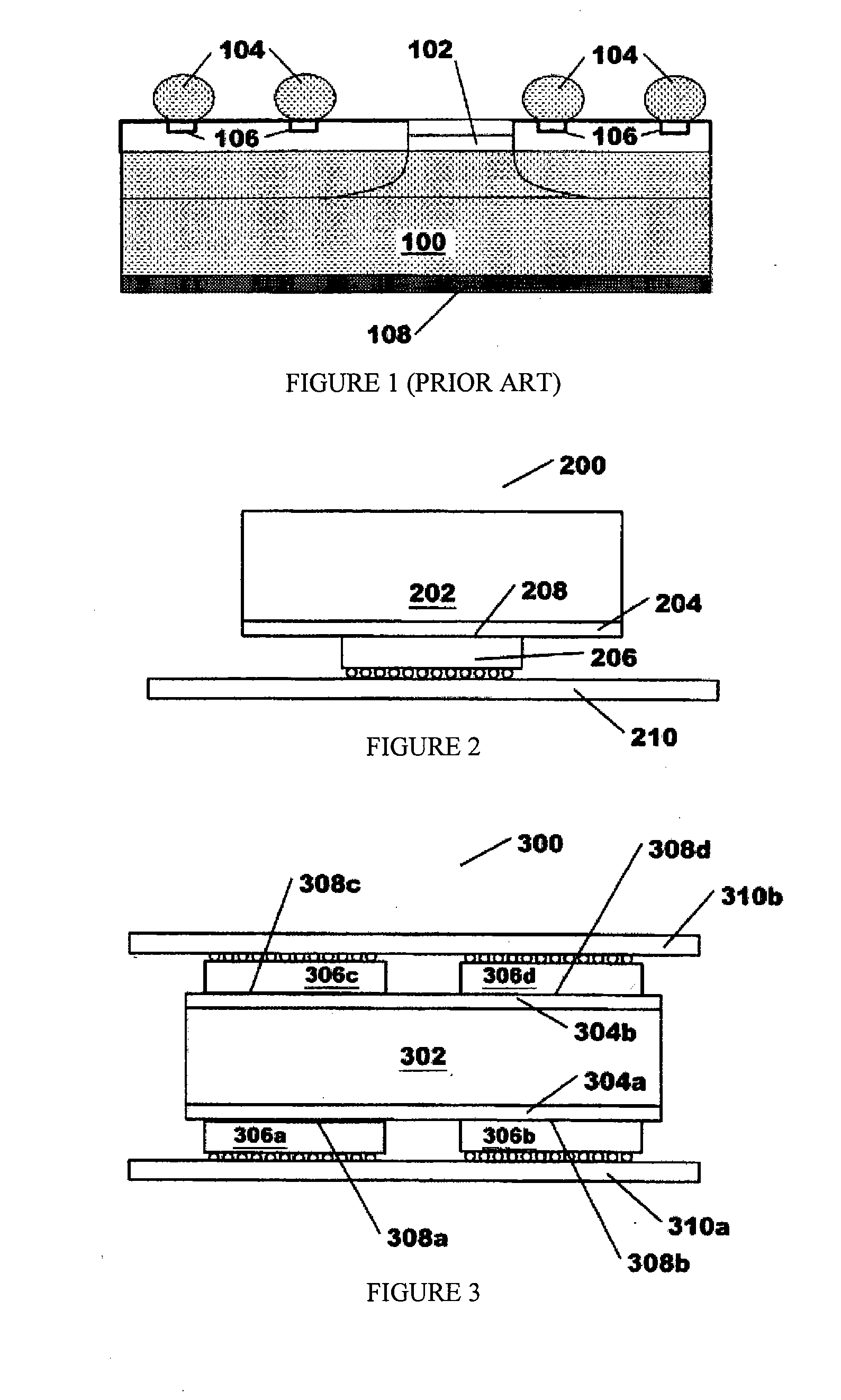
[0026]FIG. 2 is a schematic side view 200 of integrated micro-cooler device 202 attached to a flip chip integrated circuit 206 according to an embodiment of the invention. The integrated micro-cooler device 202 is a separate structure from the chip 206 that contains highly conductive, self-assembled nano structures that are integrated with heat sinking devices. It provides a low thermal resistance path for heat transferred from a surface 208 of the integrated circuit chip 206 mounted on a circuit board 210 below the thermal interface layer 204 provides a low resistance interface that contains nano-structures which enhance heat conduction from the chip 206, reduce the impact of local hot spots in the chip 206, and laterally conduct heat to a heat sink structure 202 having a greater footprint than that of the chip 206. Structural details of micro-cooler device 202 are disclosed below. The chip 206 and micro-cooler 202 may be bonded together using eutectic layers or thermal bonding adh...


PUM

PropertyMeasurementUnit
temperaturesaaaaaaaaaa
thicknessaaaaaaaaaa
thicknessaaaaaaaaaa

Abstract

Heat sink structures employing carbon nanotube or nanowire arrays to reduce the thermal interface resistance between an integrated circuit chip and the heat sink, where the nanotubes are cut to essentially the same length over the surface of the structure, are disclosed. Carbon nanotube arrays are combined with a thermally conductive metal filler disposed between the nanotubes. This structure produces a thermal interface having high axial and lateral thermal conductivities.

Description

CROSS REFERENCE TO RELATED APPLICATIONS [0001] This application is a continuation-in-part of U.S. patent application Ser. No. 10 / 925,824 now U.S. Pat. No. 7,109,581, the entirety of which is incorporated herein by this reference thereto.BACKGROUND OF THE INVENTION [0002] 1. Field of the Invention [0003] The invention relates to the removal of heat generated by an integrated circuit and the components used in chip assembly and packaging to facilitate said heat removal. More specifically, the invention discloses the application of self-assembled nano-structures for improving the performance of heat sink structures coupled to integrated circuit devices, and more specifically to a method for ensuring that a maximum number of carbon nanotubes reach contact to a cooling surface to establish a maximum contact to the surface. [0004] 2. Discussion of the Prior Art [0005] Prior art techniques that are used to cool semiconductor ICs incorporate the use of large and expensive chip packaging hav...

Claims


Application Information

Patent Timeline
Patent Type & Authority Applications(United States)
IPC IPC(8): H01L23/34
CPCB82Y10/00H01L23/373H01L2224/16H01L2224/73253H01L2924/01057H01L2924/01078H01L2924/01079H01L2924/01019H01L2924/01322H01L2924/10253H01L2924/00
Inventor DANGELO, CARLOSOLSON, DARIN
Owner NANOCONDUCTION
Why Eureka
Try Eureka