Light emitting device and method for manufacturing light emitting device
a technology manufacturing methods, which is applied in the direction of discharge tubes/lamp details, discharge tubes luminescnet screens, electric discharge lamps, etc., can solve the problems of inability to use devices in continuous use applications, insufficient heat dissipation, and high manufacturing costs of light emitting devices such as these, and achieve high reliability, thin and compact
- Summary
- Abstract
- Description
- Claims
- Application Information
AI Technical Summary
Benefits of technology
Problems solved by technology
Method used
Image
Examples
example 1
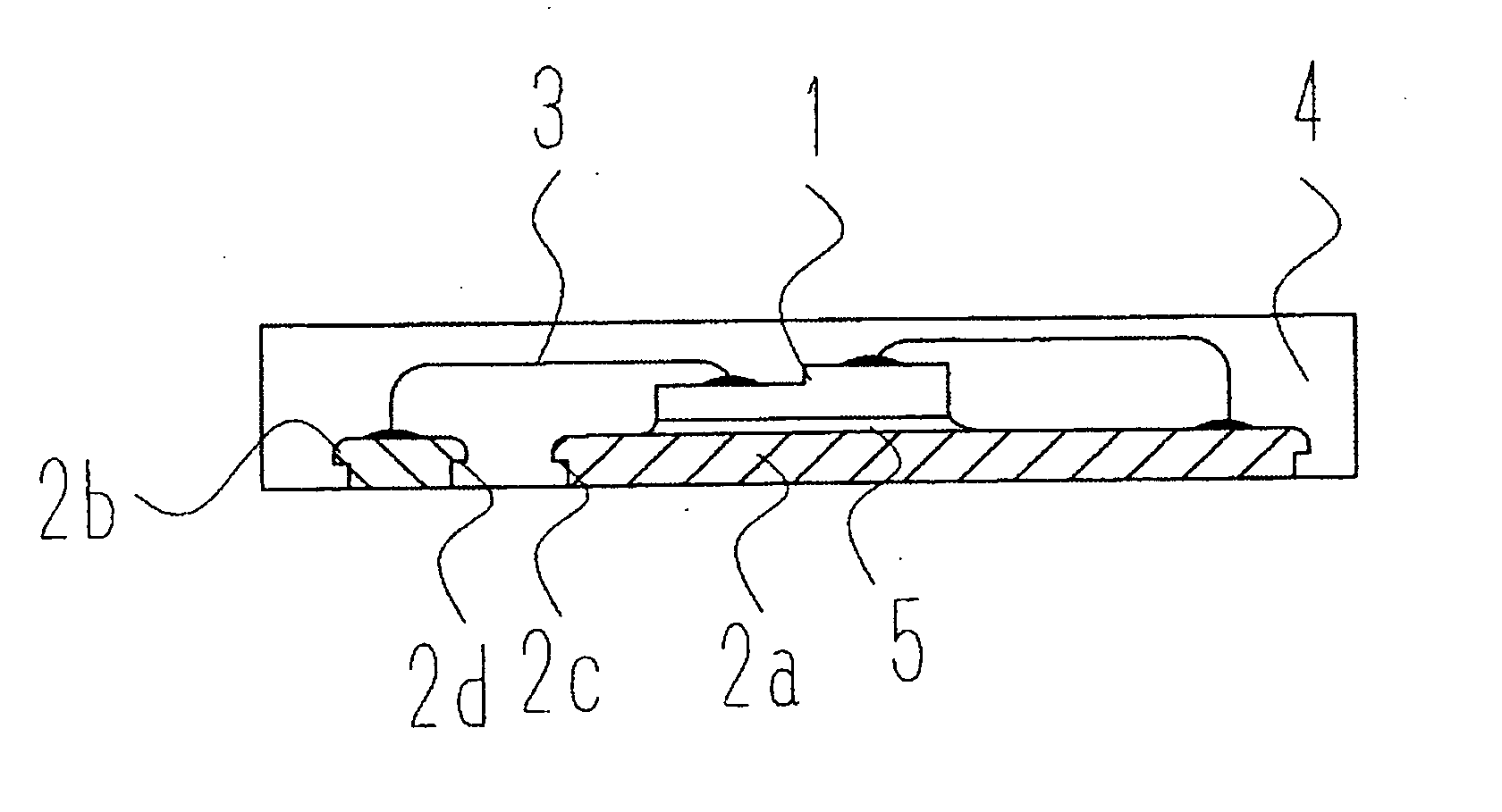
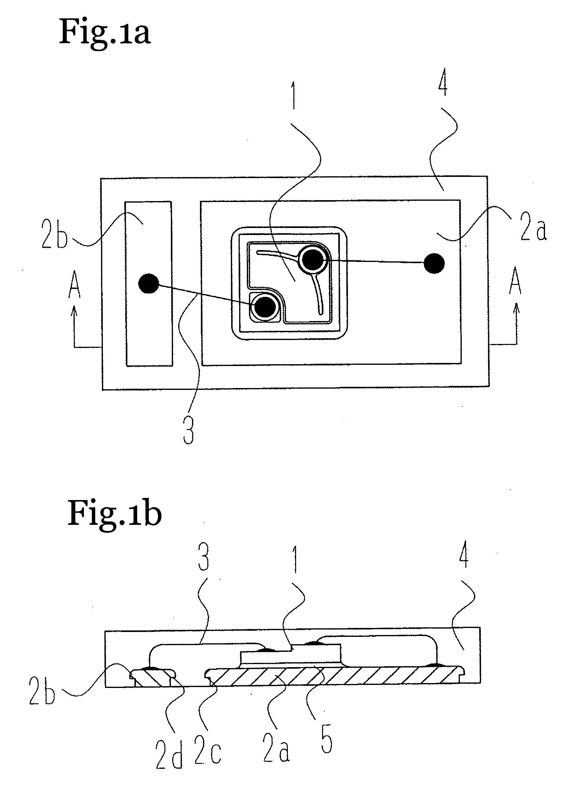
[0054] Using strip-shaped SUS 430 with a thickness of 60 μm as the metal matrix material, an intermediate layer composed of titanium was formed on the upper face of this metal matrix material, and this product was heat treated in a hydrogen gas atmosphere.
[0055] Next, a resist was formed in a thickness of 70 μm, and the resist was patterned so that an opening measuring 0.5×0.2 mm and an opening measuring 0.5×1.0 mm were arranged in parallel at a pitch of 0.2 mm.
[0056] A gold / nickel layer was formed in the openings. The upper face of the nickel layer was formed lower than the upper face of the resist. The gold layer was then formed so as to be higher than the resist upper face. The gold layer (the topmost layer) was then silver plated.
[0057] Finally, the resist was removed to obtain electroconductive layers 2a and 2b having protrusions 2c and 2d with a thickness and protruding length of 50 μm each.
[0058] Then, a light emitting element 1 was electrically connected to the pair of e...
example 2
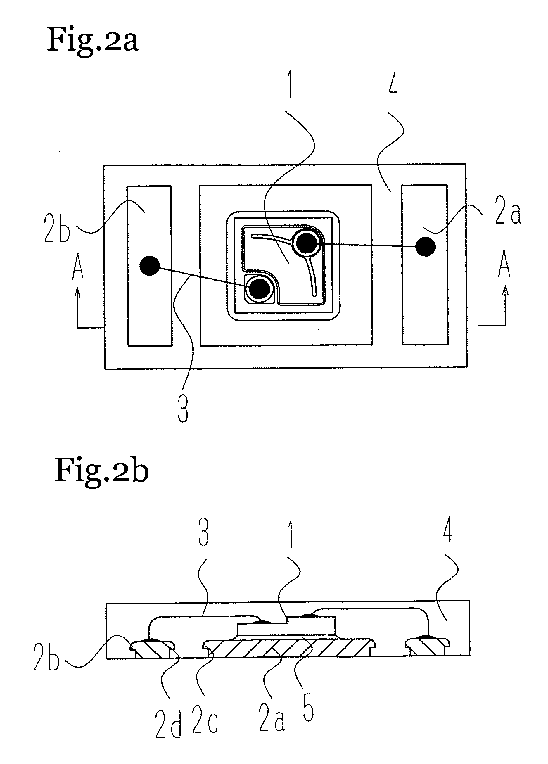
[0063] The light emitting device shown in FIG. 2 was obtained in the same manner as in Example 1, except that the resist was patterned so that an opening measuring 0.5×0.2 mm, an opening measuring 0.5×1.0 mm, and an opening measuring 0.5×0.2 mm were arranged in parallel at a pitch of 0.2 mm, there were two electroconductive layers for wire bonding in one light emitting device, and there was one electroconductive layer for holding the light emitting element. The light emitting device obtained in this manner had better heat dissipation than the one in FIG. 1.
example 3
[0064] A plurality of recesses were formed to a depth of 80 μm by etching ahead of time in the metal matrix material, and an electroconductive layer 2a equipped with a recess capable of holding a light emitting element 1 was formed.
[0065] Next, the light emitting element 1 was placed in the above-mentioned recess, and the electrodes of the light emitting element 1 were electrically connected by wires 3 to the electroconductive layers 2a and 2b, after which the recess was filled with a color conversion member 6 containing a fluorescent substance capable of absorbing light from the light emitting element and converting it to a longer wavelength. More specifically, a silicone resin and a (Y0.8Gd0.2)3Al5O12:Ce0.03 fluorescent substance were mixed in a weight ratio of 100:15 with stirring, and the recess was filled with the resulting mixture and left for 4 hours, allowing the fluorescent substance to settle. The fill amount is preferably enough to produce a shape that will protrude in t...
PUM
 Abstract
Description
Claims
Application Information


