Semiconductor device having a molded package

a semiconductor device and package technology, applied in semiconductor devices, semiconductor/solid-state device details, electrical apparatus, etc., can solve the problems of low heat dissipation effect, inability and difficulty in performing electrical grounding and heat dissipation separately from each other, so as to improve high-frequency characteristics and improve heat dissipation effect.

Active Publication Date: 2007-06-14
MITSUBISHI ELECTRIC CORP
View PDF15 Cites 9 Cited by
  • Summary
  • Abstract
  • Description
  • Claims
  • Application Information

AI Technical Summary

Benefits of technology

[0010] In view of the above-described problems, an object of the present invention is to provide a molded package having an improved heat dissipation effect and improved high-frequency characteristics and capable of performing electrical grounding and heat dissipation separately from each other.

Problems solved by technology

In these molded packages, however, the lead electrodes usually have a small thickness of about 0.2 mm and a small heat capacity and, therefore, the heat dissipation effect is low and there is a need for a heat sink of a large heat capacity for limiting the increase in temperature of the semiconductor chip.
Also, the high-frequency characteristics cannot be improved because the parasitic inductance and parasitic capacitance are increased.
In the conventional molded packages, however, it is difficult to perform electrical grounding and heat dissipation separately from each other.

Method used


Image

  • Semiconductor device having a molded package
  • Semiconductor device having a molded package
  • Semiconductor device having a molded package

Examples


first embodiment

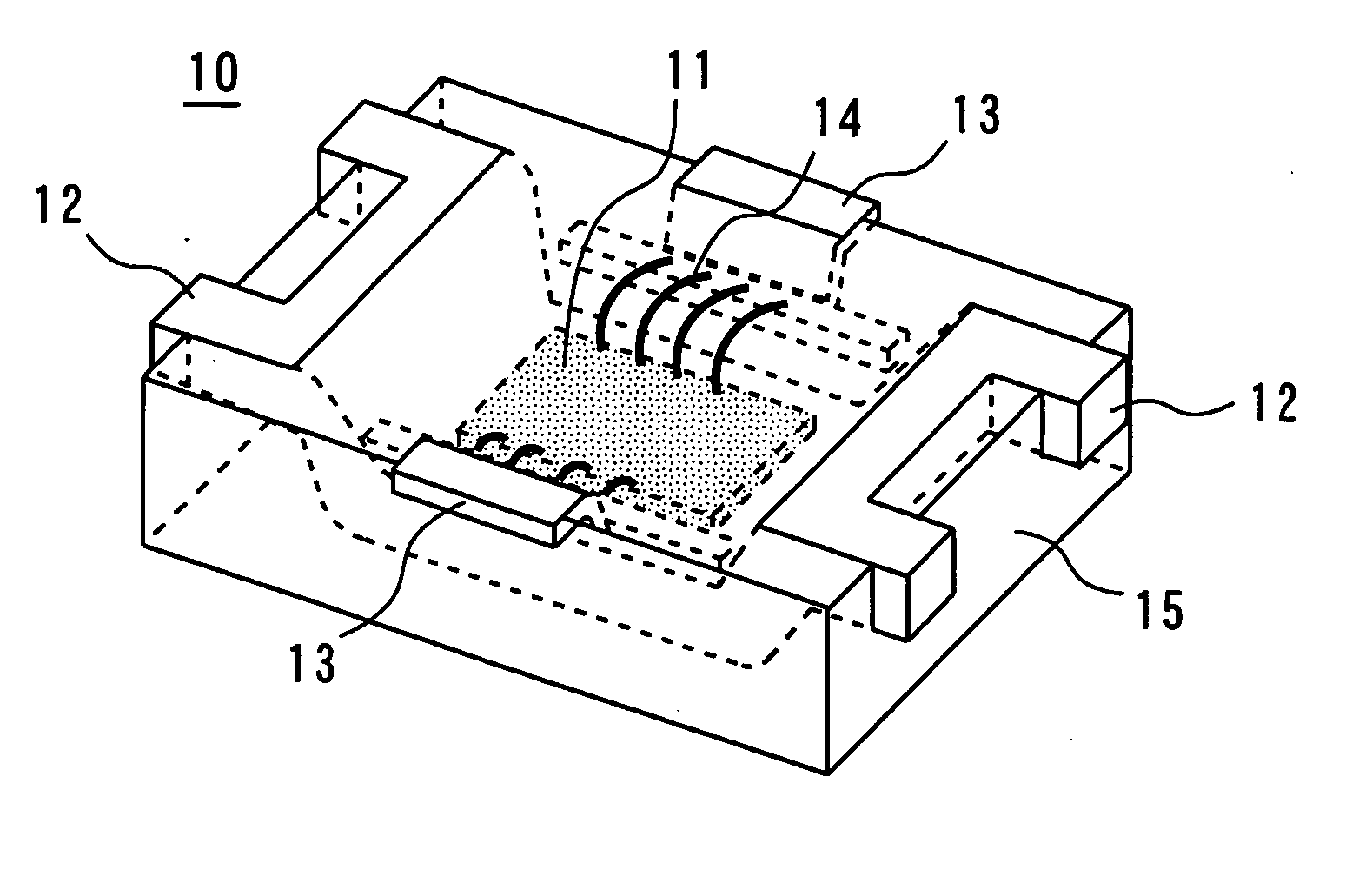
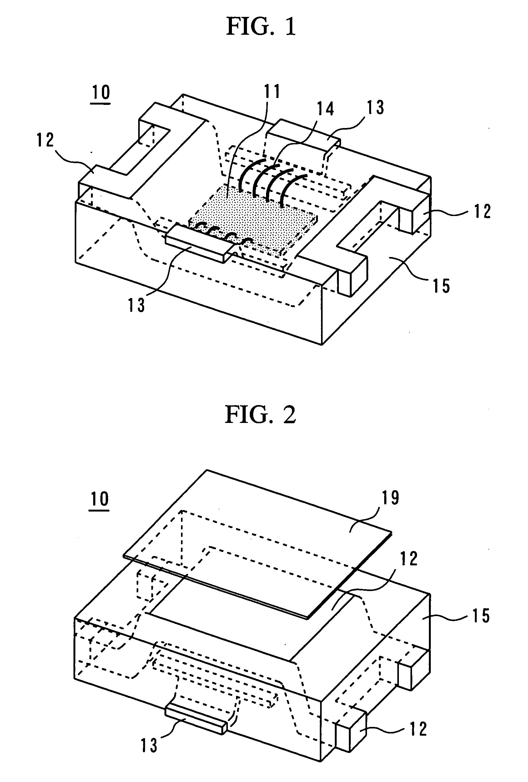
[0030]FIG. 1 is a perspective view showing a molded package according to a first embodiment of the present invention. FIG. 2 shows a state in which the molded package shown in FIG. 1 is placed upside down. As illustrated, a semiconductor chip 11 is die-bonded, for example, by soldering to a recessed portion of a thick-film lead electrode 12 having a thickness of about 0.4 to 1.0 mm. The recessed portion is formed by bending the thick-film lead electrode 12 on opposite sides of a central portion of the thick-film lead electrode 12. Thin-film lead electrodes 13 having a thickness of about 0.05 to 0.2 mm are bent downward so as to be closer to the semiconductor chip 11 and are electrically connected to the semiconductor chip by metal wires 14. The semiconductor chip 11 and the metal wires 14 are encapsulated in a molding material 15 such as a plastic to form a molded package 10.

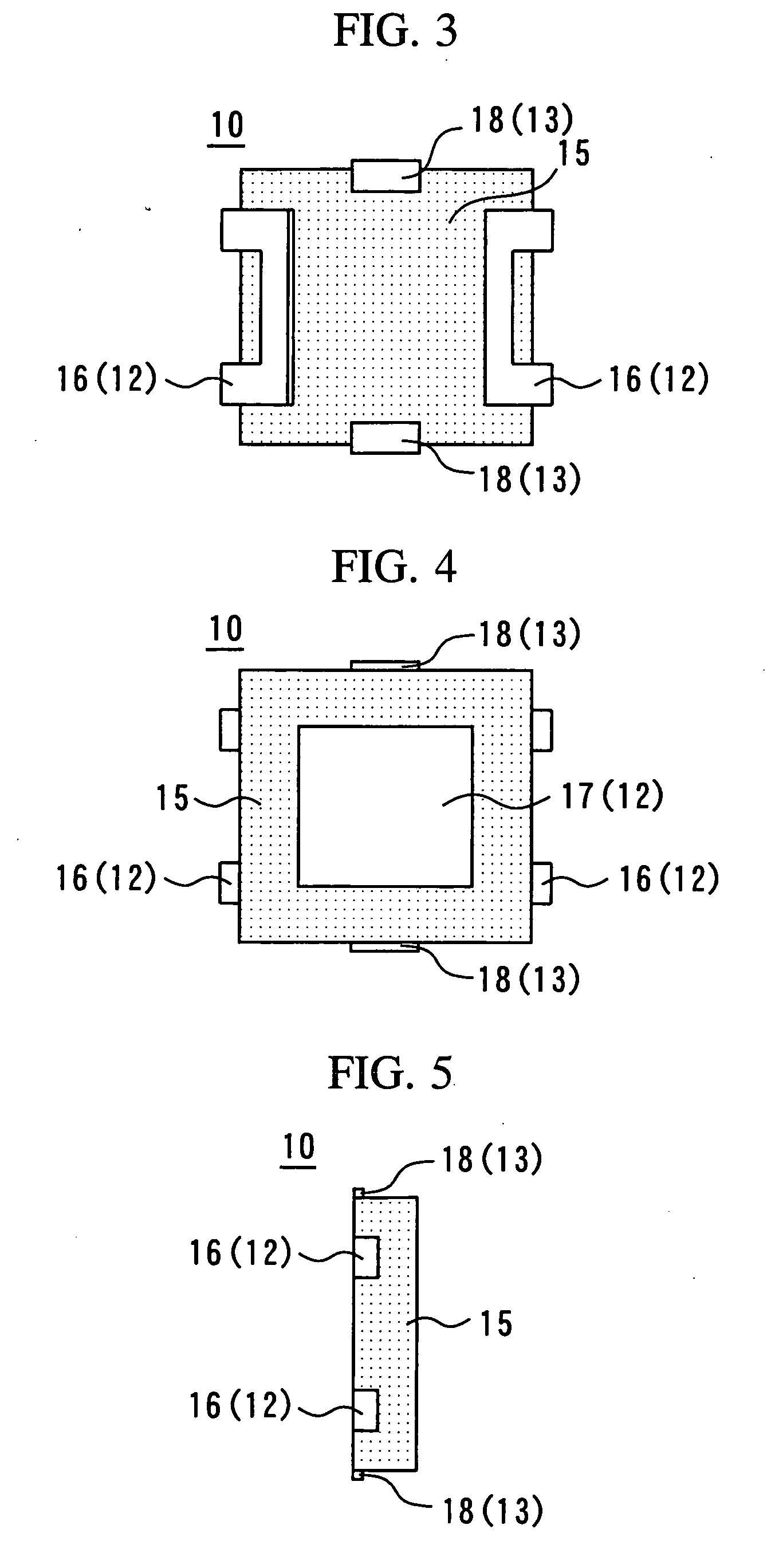
[0031]FIG. 3 shows a top view of this molded package; FIG. 4 a bottom view; and FIG. 5 a side view. As illus...

second embodiment

[0044]FIG. 11 is a sectional view showing a molded package according to a second embodiment of the present invention. Constituents identical or corresponding to those shown in FIGS. 1 through 10 are indicated by the same reference numerals and the description for them will not be made.

[0045] In the molded package according to this embodiment, a copper oxide film 27 is precipitated on a plating layer 24 formed by plating with silver (Ag) for example. The closeness of contact between the thick-film lead electrode 21 and the molding material 15 in the vicinity of the semiconductor chip 11 is thereby improved to further improve the reliability of the semiconductor chip 11.

[0046] As a method for precipitation of the copper oxide film 27 on the plating layer 24, a method may be used in which the surface of the thick-film lead electrode 21 is oxidized in an atmosphere in which the proportion of an inert gas such as nitrogen (N2) is high to cause copper oxide formed on the surface of the ...


PUM


Abstract

A semiconductor device having a molded package includes a semiconductor chip, a thick-film lead electrode to which the semiconductor chip is die-bonded, a thin-film lead electrode having a thickness smaller than that of the thick-film lead electrode, a wire which electrically connects the semiconductor chip to the thin-film lead wire, and a molding material in which the semiconductor chip and the wire are encapsulated. A portion of a lower surface of the thick-film lead electrode is exposed at a package lower surface as a heat dissipating electrode. A portion of an upper surface of the thin-film lead electrode is exposed at a package upper surface as an input/output electrode. A portion of an upper surface of the thick-film lead electrode is exposed at the package upper surface as a grounding electrode.

Description

BACKGROUND OF THE INVENTION [0001] 1. Field of the Invention [0002] The present invention relates to a molded package operating at a high frequency or a high output and, more particularly, to a molded package having an improved heat dissipation effect and improved high-frequency characteristics and capable of performing electrical grounding and heat dissipation separately from each other. [0003] 2. Background Art [0004]FIG. 12 shows an example of a conventional molded package operating at a high frequency or a high output (see, for example, Japanese Patent Laid-Open No. 8-213536). As illustrated, thin-film lead electrodes 51 are bent downward to form input / output lead electrodes 52. Also, the thin-film lead electrodes 51 are bent upward to form die pad portions 53 to which a semiconductor chip 54 is bonded, for example, by soldering. The semiconductor chip 54 is connected to the input / output lead electrodes 52 through metal wires 56. The semiconductor chip 54 and the metal wires 56 ...

Claims


Application Information

Patent Timeline
Patent Type & Authority Applications(United States)
IPC IPC(8): H01L23/28
CPCH01L23/3135H01L23/49537H01L23/49551H01L23/66H01L2224/48091H01L2224/48247H01L2224/49171H01L2224/49175H01L2924/01078H01L2924/1532H01L2924/30107H01L2924/00014H01L24/48H01L24/49H01L2924/00H01L2224/451H01L24/45H01L2924/181H01L2924/00015H01L2924/00012
Inventor FUJITA, KOICHIMARUYAMA, YOJIHINO, KENJI
Owner MITSUBISHI ELECTRIC CORP
Why Eureka
Try Eureka