
Method for Manufacturing Ferroelectric Memory

a technology of ferroelectric memory and manufacturing method, which is applied in the direction of capacitors, semiconductor devices, electrical apparatus, etc., can solve the problems of difficult to completely prevent deterioration, insufficient consideration of transistor reliability, and insufficient influence of the ferroelectric layer, so as to improve the reliability of the ferroelectric capacitor. , the effect of affecting the ferroelectric layer

Inactive Publication Date: 2007-06-14
SEIKO EPSON CORP
View PDF15 Cites 35 Cited by
  • Summary
  • Abstract
  • Description
  • Claims
  • Application Information

AI Technical Summary

Benefits of technology

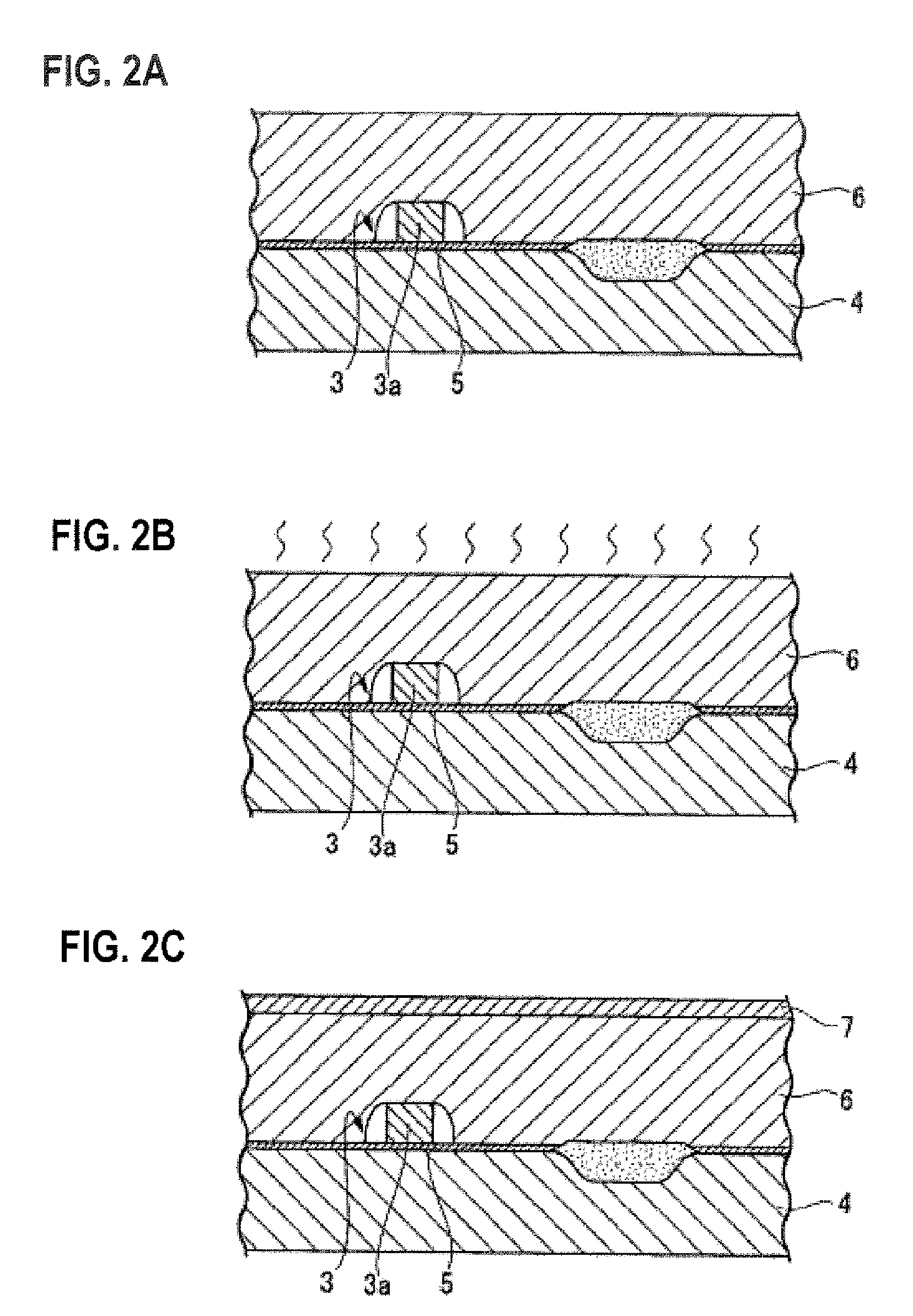
[0011] In accordance with an advantage of some aspects of the present invention, it is possible to provide a method for manufacturing a ferroelectric memory, which can achieve both prevention of deterioration of ferroelectric layers and desired effects of hydrogen sintering treatment on transistors.
[0013] According to the method for forming a ferroelectric memory described above, after the driving transistor has been formed, hydrogen sintering treatment is conducted prior to forming the first hydrogen barrier film, such that the hydrogen sintering treatment can be applied to the driving transistor without being influenced by the hydrogen barrier film, and therefore the interface state in the gate oxide film can be stabilized (reduced).
[0015] When hydrogen sintering treatment is directly applied to the driving transistor, there is a possibility of negatively affecting a semiconductor region composing the driving transistor, for example, impurity regions such as source / drain regions. However, by conducting the hydrogen sintering treatment after forming the first interlayer dielectric film, the possibility can be reduced. In other words, by applying the hydrogen sintering treatment indirectly to the driving transistor through the first interlayer dielectric film, hydrogen existing in the first interlayer dielectric film is excited, and the hydrogen can be made to act on the driving transistor, whereby the effects on the gate dielectric film can be maintained, and negative effects on the semiconductor regions can be reduced.
[0017] As a result, conditions of the interface between the plug and the wiring can be made better by the hydrogen sintering treatment, and the contact resistance can be reduced. Also, the second hydrogen barrier film is formed in a manner to cover the ferroelectric capacitor, such that the effects of the hydrogen sintering treatment can be prevented from reaching the ferroelectric capacitor.
[0019] As a result, influences on the ferroelectric layer in the ferroelectric capacitor, which may be caused by hydrogen in the second interlayer dielectric film, can be reduced, and therefore the reliability of the ferroelectric capacitor can be improved.

Problems solved by technology

However, when areas around the ferroelectric capacitor are covered by the hydrogen barrier film as described above, the hydrogen sintering treatment in the final step would not effectively act on the driving transistor due to the function of the hydrogen barrier film, which causes a problem in particular in that the interface state in the gate dielectric film would not sufficiently be reduced.
However, even when ferroelectric films per se are improved so as to be resistive to deterioration by hydrogen, it is very difficult to completely prevent deterioration.
For example, the aforementioned document describes prevention of deterioration of ferroelectric films, but hardly discusses sintering effects on transistors, and therefore may not give sufficient consideration to the reliability of transistors.
When hydrogen sintering treatment is directly applied to the driving transistor, there is a possibility of negatively affecting a semiconductor region composing the driving transistor, for example, impurity regions such as source / drain regions.

Method used


Image

  • Method for Manufacturing Ferroelectric Memory
  • Method for Manufacturing Ferroelectric Memory
  • Method for Manufacturing Ferroelectric Memory

Examples


Embodiment Construction

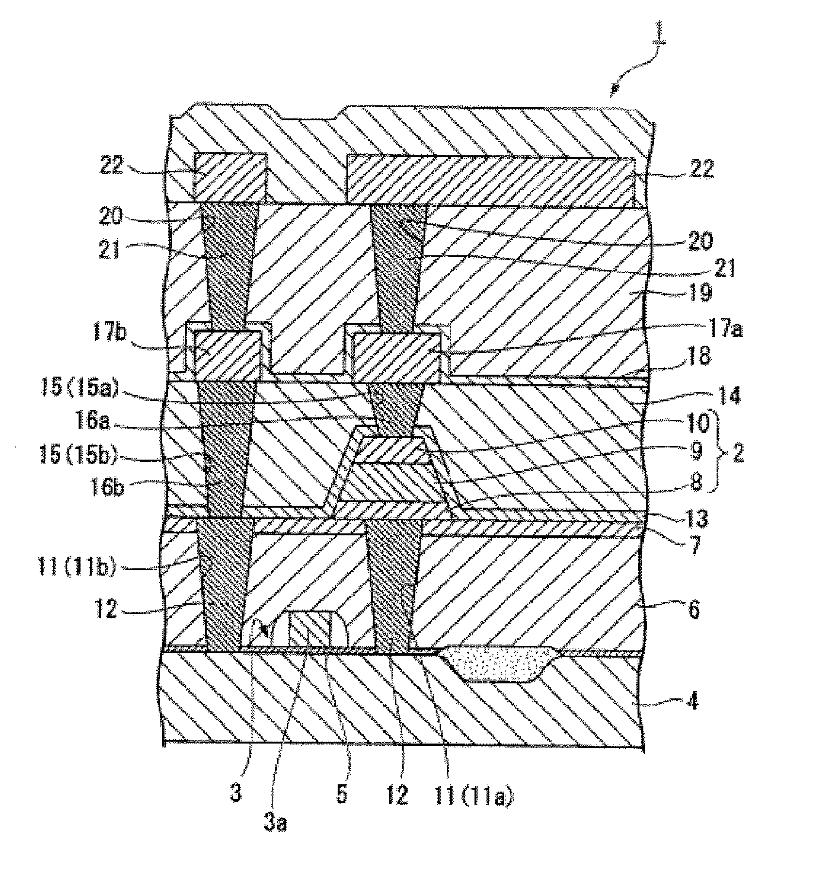
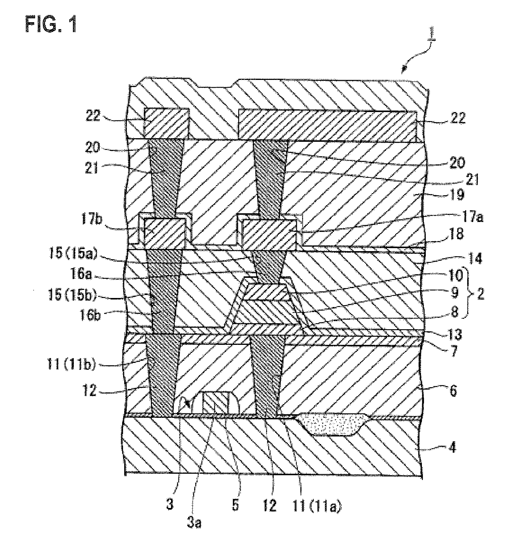
[0024] Preferred embodiments of the invention are described below in detail. Prior to describing a method for manufacturing a ferroelectric memory in accordance with an embodiment of the invention, an example of a ferroelectric memory in accordance with an embodiment of the invention is described. FIG. 1 is a cross-sectional view of a main portion of a ferroelectric memory in accordance with the embodiment of the invention. and the reference numeral 1 in FIG. 1 denotes the ferroelectric memory. The ferroelectric memory 1 is equipped with a ferroelectric capacitor 2, and a driving transistor 3 for operating the ferroelectric capacitor 2, wherein the driving transistor 3 is formed on a semiconductor substrate 4.

[0025] The semiconductor substrate 4 is composed of a silicon substrate, and has source / drain regions (not shown) and a channel region (not shown) formed in its surface section, and a gate dielectric film 5 formed on the channel region. Further, a gate electrode 3a is formed o...


PUM


Abstract

A method for manufacturing a ferroelectric memory includes the steps of forming a driving transistor on a semiconductor substrate, forming a first interlayer dielectric film that covers the driving transistor on the semiconductor substrate, forming a first hydrogen barrier film on the first interlayer dielectric film, and forming a ferroelectric capacitor electrically connected to the driving transistor on the first hydrogen barrier film, wherein hydrogen sintering treatment is conducted between the step of forming the driving transistor and the step of forming the first hydrogen barrier film.

Description

[0001] The entire disclosure of Japanese Patent Application No. 2005-343343, filed Nov. 29, 2005 is expressly incorporated by reference herein. BACKGROUND [0002] 1. Technical Field [0003] The present invention relates to a method for manufacturing a ferroelectric memory having a ferroelectric capacitor. [0004] 2. Related Art [0005] A ferroelectric memory, for example, a ITIC type ferroelectric memory is equipped with a ferroelectric capacitor and a driving transistor for driving the ferroelectric capacitor. In general, in the process of manufacturing ferroelectric capacitors, it is an important task to prevent deterioration of ferroelectric layers. More specifically, in the process of manufacturing a ferroelectric capacitor, after a ferroelectric layer is formed, the ferroelectric layer may be exposed to a hydrogen atmosphere (i.e., a reducing atmosphere) in the steps of forming an interlayer dielectric film, dry-etching and the like. When the ferroelectric layer is exposed to a red...

Claims


Application Information

Patent Timeline
IPC IPC(8): H01L21/00
CPCH01L21/76895H01L27/11502H01L27/11507H01L28/57H10B53/30H10B53/00
Inventor NODA, TAKAFUMI
Owner SEIKO EPSON CORP
Learn More