Semiconductor element and method of making same

a semiconductor and element technology, applied in the field of semiconductor element making methods, can solve the problems of difficult to break the wafer into dice, difficult to break the wafer at a high product yield by the dicing process, and the substrate may be peeled off to damage the die, etc., and achieve the effect of high product yield

Inactive Publication Date: 2007-06-14
TOYODA GOSEI CO LTD +1
View PDF8 Cites 47 Cited by
  • Summary
  • Abstract
  • Description
  • Claims
  • Application Information

AI Technical Summary

Benefits of technology

[0014] It is an object of embodiments according to the invention to provide a method of making a semiconductor element that can produce the semiconductor element (i.e., chip), which c

Problems solved by technology

However, since the sapphire substrate is not conductive, the light emitting element need have a horizontal electrode structure which requires an etching process after the formation of a semiconductor layer on the substrate.
Thus, when the wafer is divided into dice, the substrate may be peeled off to damage the die.
In other words, it is difficult to break the wafer into dice even though a high-quality group III nitride-based compound semiconductor layer can be formed on the substrate.
Thus, since the gallium o

Method used


Image

  • Semiconductor element and method of making same
  • Semiconductor element and method of making same
  • Semiconductor element and method of making same

Examples


first embodiment

[0071] A method of making a semiconductor element in the first embodiment will be explained below.

[0072] Formation of Semiconductor Layer

[0073] A wafer of β-Ga2O3 is placed in an MOCVD apparatus and its surface is at first nitrided. The nitriding method is not specifically limited and, for example, the wafer of β-Ga2O3 may be heated in ammonium atmosphere. Then, group III nitride-based compound semiconductor layers are on its (100)-plane by an ordinary method.

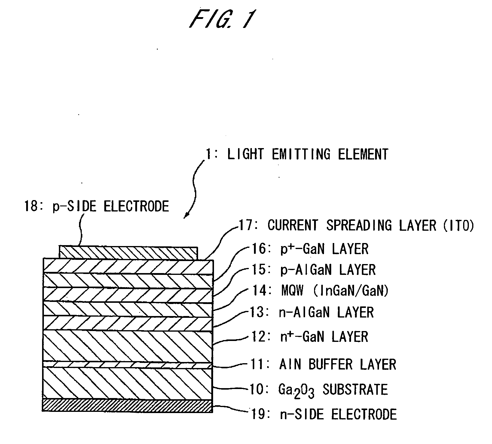
[0074] In this embodiment, the semiconductor element has a layer structure as mentioned below so as to compose a light emitting element (or LED element) (See FIG. 1). FIG. 1 is illustrated to show the layer structure and does not precisely show the film thickness of each layer thereof.

LayerCompositionp-contact layer 16p+-GaNp-cladding layer 15p-AlGaNMQW light emitting layer 14InGaN / GaNn-cladding layer 13n-AlGaNn-contact layer 12n+-GaNbuffer layer 11AlxGa1−xN (0.5 ≦ x ≦ 1)substrate 10β-Ga2O3

[0075] As described earlier, the ...

second embodiment

[0095] Gallium Oxide Substrate

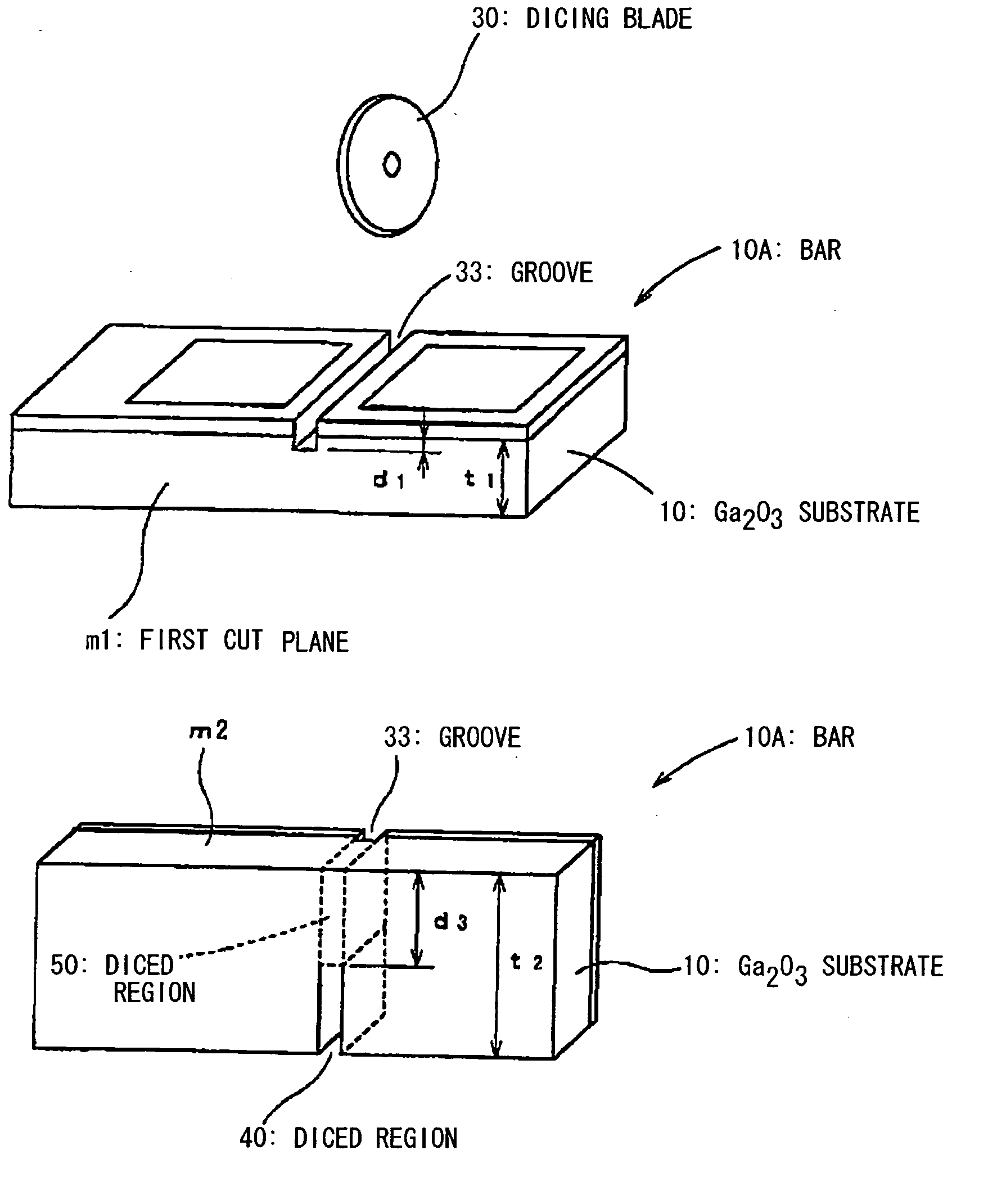
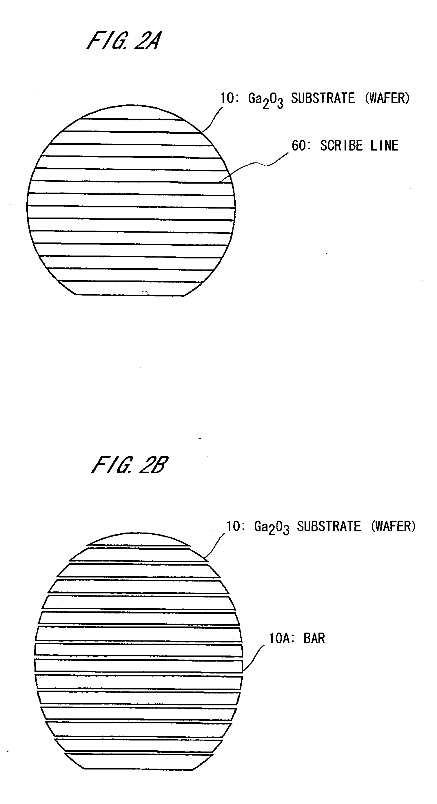
[0096]FIG. 6 shows the gallium oxide substrate on which a light emitting element (LED element) is formed.

[0097] The β-Ga2O3 substrate 10 as the gallium oxide substrate is a substrate that is processed into a wafer with a predetermined plane direction. In case of the β-Ga2O3 substrate 10, the substrate surface is set (100), (010), (001)-plane or (801)-plane, and has a strong cleavage property at the (100)-plane. As described above, when the substrate surface is set (100), (010), (001)-plane or (801)-plane, the cleavage property is also recognized at the (001)-plane.

[0098] In growing the light emitting element on the β-Ga2O3 substrate 10, the substrate surface is set the (100)-plane or (801)-plane so as to facilitate the wafer processing and the formation of the light emitting element. In this case, the wafer is cleaved along the (001)-plane by using the cleavage property and cut along the (010)-plane by dicing etc., so that a number of the light emitt...

third embodiment

[0132]FIG. 1 is a cross sectional view showing a nitride semiconductor element, i.e., a group III nitride-based compound semiconductor light emitting element (hereinafter simply called ‘light emitting element’), in the third preferred embodiment of the invention.

[0133] Structure of Light Emitting Element

[0134] The light emitting element 1, which is a vertical type light emitting element with p- and n-side electrodes disposed in vertical direction, comprises: a Ga2O3 substrate 10 as a growth substrate for growing group III nitride-based compound semiconductor thereon; and, sequentially formed on the Ga2O3 substrate 10, an AlN buffer layer 11; a Si-doped n+-GaN layer 12; a Si-doped n-AlGaN layer 13; MQW (multiquantum well) 14 with a multiquantum well structure formed of InGaN / GaN; a Mg-doped p-AlGaN layer 15; a Mg-doped p+-GaN layer 16; and a current spreading layer 17 formed of ITO (indium tin oxide) to spread current into the p+-GaN layer 16. The AlN buffer layer 11 to the p+-GaN ...


PUM


Abstract

A method of making a semiconductor element which has a substrate formed of gallium oxide and a semiconductor layer formed on the substrate. The method has: a first dividing step that the substrate with the semiconductor layer formed thereon is divided into a strip bar along a first cleaved surface of the substrate; and a second dividing step that the strip bar is divided in a direction perpendicular to the first cleaved surface.

Description

[0001] The present application is based on Japanese patent application Nos. 2005-360441, 2006-055332 and 2006-187478, the entire contents of which are incorporated herein by reference. BACKGROUND OF THE INVENTION [0002] 1. Field of the Invention [0003] This invention relates to a method of making a semiconductor element and, in particular, to a method of making a semiconductor element (chip) comprising a gallium oxide (Ga2O3) substrate and a semiconductor layer formed thereon. Also, this invention relates to the semiconductor element made by using the method. [0004] 2. Description of the Related Art [0005] Group III nitride-based compound semiconductors are used for the manufacture of a short-wavelength light emitting element (or LED element). Such a light emitting element uses a transparent sapphire substrate. However, since the sapphire substrate is not conductive, the light emitting element need have a horizontal electrode structure which requires an etching process after the for...

Claims


Application Information

Patent Timeline
IPC IPC(8): H01L21/00
CPCH01L21/02414H01L21/02458H01L21/02505H01L21/0254H01L21/02579H01L21/02658H01L21/02664H01L21/78H01L33/0095
Inventor IKEMOTO, YUHEIHIRATA, KOJIAOKI, KAZUOKANEKO, YUKIOUJIIE, TAKEKAZU
Owner TOYODA GOSEI CO LTD
Why Eureka
Try Eureka