Method for manufacturing ic-embedded substrate

a technology of ic-embedded substrates and manufacturing methods, which is applied in the direction of etching metal masks, conductive pattern formation, lithographic masks, etc., can solve the problems of high precision of processing, high yield, and damage to semiconductor ic chips, so as to achieve the effect of increasing reducing the number of processing holes, and not reducing productivity

Active Publication Date: 2007-06-21
TDK CORPARATION
View PDF5 Cites 29 Cited by
  • Summary
  • Abstract
  • Description
  • Claims
  • Application Information

AI Technical Summary

Benefits of technology

[0012] In the present invention, the first step may includes a step for encapsulating not only the IC chip but other electronic components in the insulating layer, particularly chip components of a passive element. When other electronic components are encapsulated with the IC chip, the number of processing holes further increases along with the number of embedded elements, and the height of the pad electrode varies. However, according to the present invention, productivity does not decrease as the number of processing holes increases, the elements are not damaged by stress during polishing, and variation in the degree of polishing due to the differing heights of the via holes can be absorbed. In other words, the present invention is able to address the assorted problems that have accompanied increasing the number of embedded elements, which has traditionally been difficult. The passive element chip component may be a passive element unit, an array, or an RLC composite part.
[0013] According to the present invention, a semiconductor IC chip is encapsulated, conformal processing is performed, and blasting is subsequently carried out to expose a pad electrode of the semiconductor IC chip. A mask for forming via holes can accordingly be formed with high precision, and the various problems caused by laser processing can be resolved. Specifically, it is possible to prevent electronic parts being damaged by heat, keep productivity from decreasing when the number of processing holes increases, and manage fine pitch electrode arrays of semiconductor IC chips.
[0014] Further, the problems that occur when the entire surface of the insulating layer is ground by polishing or the like can be resolved as described hereinbelow. Specifically, electronic parts can be prevented from being damaged under loading (stress), variation in the degree of polishing due to the differing heights of the via holes can be absorbed because the metal layer functions as a stopper, and the range over which the degree of polishing is set can be expanded. Furthermore, the adhesive strength between the copper foil and the resin is increased; therefore, adequate wiring strength can be ensured.

Problems solved by technology

First, when a via hole is formed directly above a pad electrode of a semiconductor IC chip, the semiconductor IC chip will be damaged if the via hole is formed by laser processing in the same manner as a via hole in a regular IC substrate because the semiconductor IC chip will be directly subjected to thermal shock, and the yield will deteriorate.
Particularly, since the pad electrodes of the semiconductor IC chip are disposed at a fine pitch, the precision with which the processing is performed is necessarily very high, and certain laser devices may not be capable of such precision.
Since the number of via holes increases along with the number of pad electrodes on a semiconductor IC chip, the production capacity of the laser device inevitably fluctuates, and productivity declines.
The following problems are encountered in the method for exposing a pad electrode of a semiconductor IC chip by polishing the entire surface of an encapsulating resin layer (Japanese Patent Application Publication No. 2001-250902).
When the entire surface of the encapsulating resin is polished, the semiconductor IC chip is often damaged due to the load applied to the substrate, and a reduced yield results.
The range within which the degree of polishing can be set is limited, and it is extremely difficult to minimize polishing variation.
However, reliability declines due to the low adhesive strength between the polished resin surface and the electroless plating.
Furthermore, semiconductor IC chips embedded in substrates are different from other electronic components, and comprise many expensive parts.

Method used


Image

  • Method for manufacturing ic-embedded substrate
  • Method for manufacturing ic-embedded substrate
  • Method for manufacturing ic-embedded substrate

Examples


first embodiment

[0035] The method for manufacturing an IC-embedded substrate according to the present embodiment can be used when a semiconductor IC chip is to be mounted on a “core substrate” that constitutes an IC-embedded substrate; or when a semiconductor IC chip is to be mounted on a “build-up layer” formed on a core substrate. First, a first embodiment in which a semiconductor IC chip is mounted on a core substrate will be described in detail with reference to FIGS. 1 to 9.

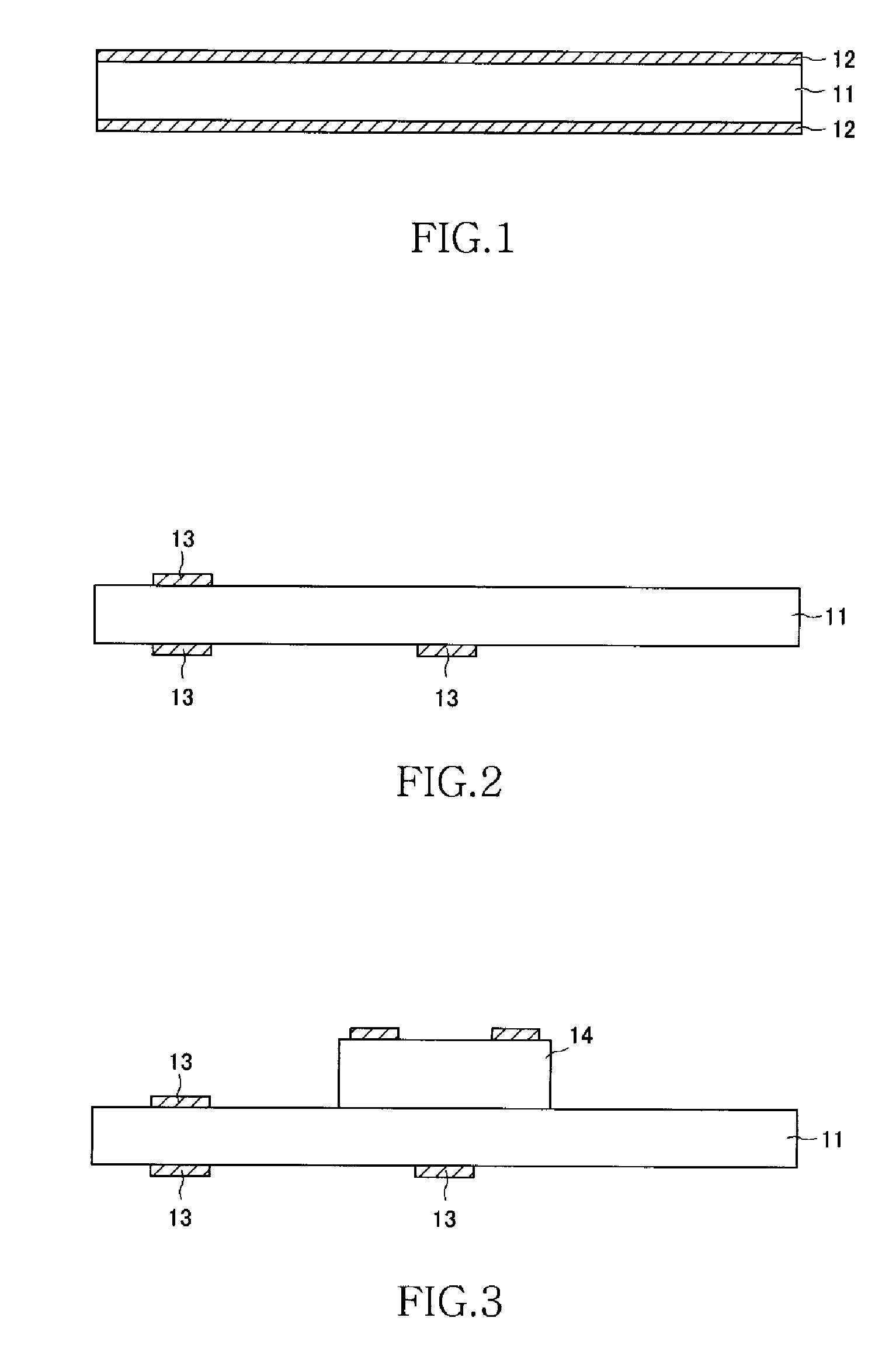
[0036] First, a core substrate 11 is prepared when an IC-embeded substrate is manufactured according to the present embodiment (FIG. 1). The core substrate 11 serves to preserve the mechanical strength of the entire IC-embedded substrate. There are no particular limitations thereto; for example, a resin substrate having a copper foil on either side thereof can be used. The material used for the resin substrate is preferably a core material comprising a glass cloth, Kevlar material, aramid, a cloth made from a liquid crystal...

third embodiment

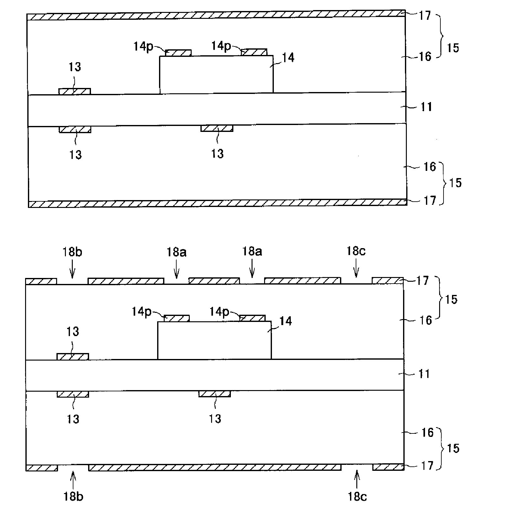
[0060] Next, the present invention will be described in detail.

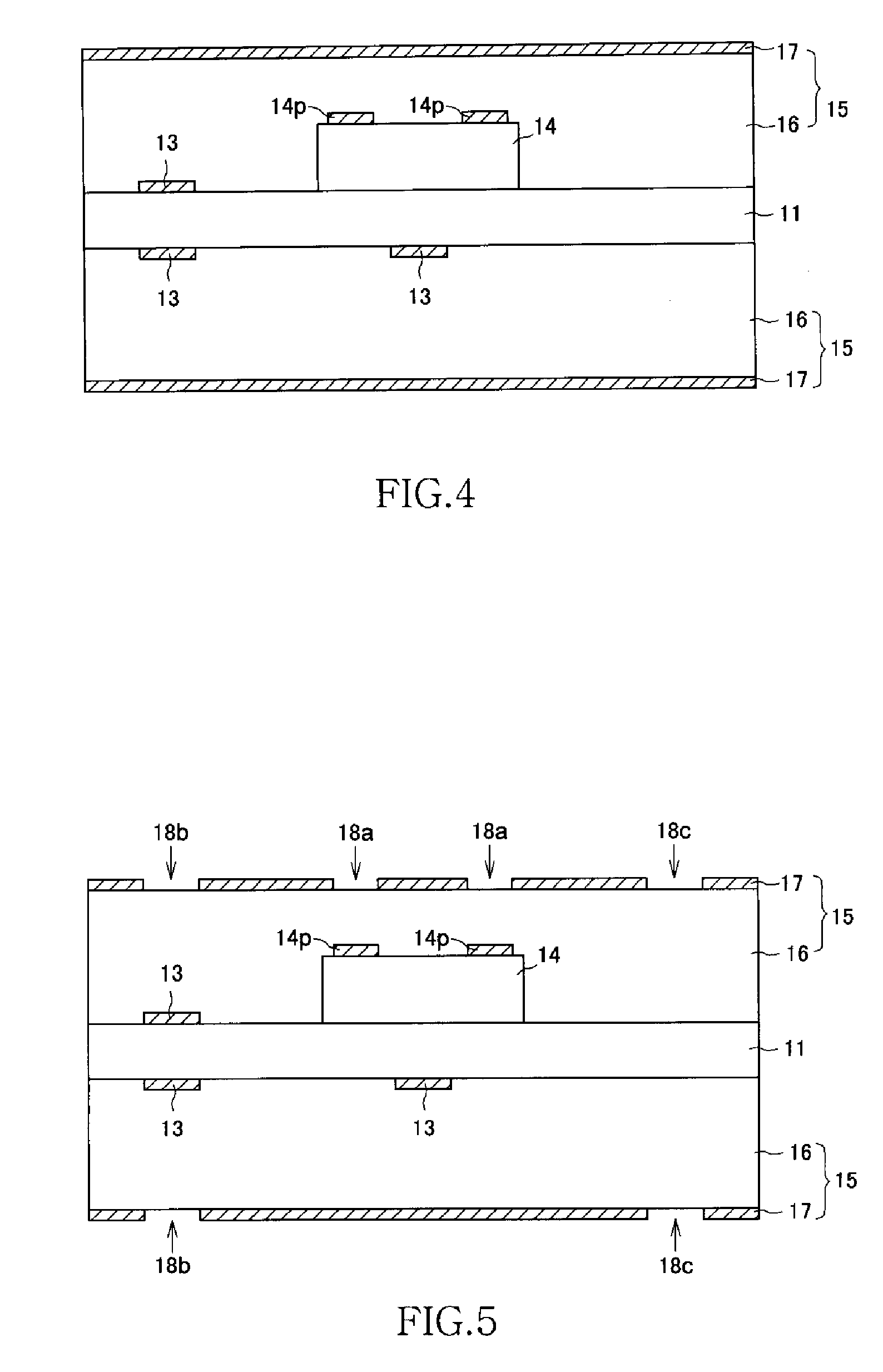
[0061] In the method for manufacturing an IC-embedded substrate according to the present embodiment, first, a core substrate 11 is prepared in the same manner as in the first embodiment described above (FIG. 11), and a copper foil 12 disposed on either side of the core substrate 11 is selectively removed by photolithography and etching, whereby a conductor pattern 13 comprising wiring and lands is formed on the core substrate 11 (FIG. 2). Next, a semiconductor IC chip 14 is mounted face up in a prescribed region on the core substrate 11 (FIG. 3), and resin sheets 15 having a copper foil on one side thereof are affixed to either side of the core substrate 11 on which the semiconductor IC chip 14 has been mounted (FIG. 4). Thus, the copper foil 17 formed on the surface of the build-up layer is selectively removed by conformal processing, whereby a mask pattern for forming the via holes is formed (FIG. 5). An aperture patte...


PUM

PropertyMeasurementUnit
thicknessaaaaaaaaaa
thicknessaaaaaaaaaa
diameteraaaaaaaaaa

Abstract

A method for manufacturing an IC-embedded substrate comprises a first step for encapsulating at least an IC chip having a pad electrode in an insulating layer, a second step for forming a metal layer having at least a first aperture in a location directly above the pad electrode of the IC chip and a second aperture in a location above an area other than the area in which the IC chip is mounted, and a third step for selectively removing the insulating layer by a blasting treatment in which the metal layer is used as a mask, whereby forming a first via hole that corresponds to the first aperture and a second via hole that corresponds to the second aperture.

Description

TECHNICAL FIELD [0001] The present invention relates to a method for manufacturing an IC-embedded substrate, and particularly relates to a method for forming via holes in a multilayer substrate in which an IC is embedded. BACKGROUND OF THE INVENTION [0002] Printed wiring boards having a highly dense mounted structure are known to have structures in which printed substrates are fashioned in multiple layers and semiconductor IC chips are embedded therein (see Japanese Patent Application Laid Open No. 2001-237347). Methods used for exposing a pad electrode of a semiconductor IC chip embedded into a printed wiring substrate include a method whereby a laser is used to form a via hole directly above the pad electrode (see Japanese Patent Application Laid Open No. 9-321408); and a method in which the entire surface of a resin layer in which the semiconductor IC chip is encapsulated is polished and the pad electrode is exposed (see Japanese Patent Application Laid Open No. 2001-250902). [00...

Claims


Application Information

Patent Timeline
Patent Type & Authority Applications(United States)
IPC IPC(8): H01L21/00
CPCH01L23/5389Y10T29/49126H01L24/82H01L25/16H01L2224/24226H01L2224/82039H01L2924/01029H01L2924/01033H01L2924/01078H01L2924/14H01L2924/30107H05K1/185H05K3/0044H05K3/4652H05K2201/0209H05K2201/09509H05K2201/09518H05K2201/10674H05K2203/025H05K2203/0554H01L2924/01005H01L2924/01006H01L2924/01043H01L2224/73267Y10T29/49128Y10T29/49139Y10T29/49155Y10T29/49151Y10T29/4913H01L24/24H01L21/3205
Inventor NAGASE, KENJIKAWABATA, KENICHI
Owner TDK CORPARATION
Why Eureka
Try Eureka