Random number generating method and semiconductor integrated circuit device

Inactive Publication Date: 2007-06-21
HITACHI ULSI SYST
View PDF8 Cites 19 Cited by
  • Summary
  • Abstract
  • Description
  • Claims
  • Application Information

AI Technical Summary

Benefits of technology

[0168] As has been described above, the true random number generating circuit according to the present inventions is entirely realized only by the standard CMOS logic circuits. This reduces the load required for a complicated analog circuit design and LSI mounting and contributes to reduction of the cost and improvement of reliability.

Problems solved by technology

However, the conventional random number generating circuits have good and bad points.
True random number has advantages of eventuality, un-reproducibility, and unpredictability but it requires a complicated circuit and element which cannot be obtained in a simple device.
Accordingly, a factor lowering the irregularity of a random number cannot be predicted at the design stage and it is difficult to guarantee the quality of the random number.

Method used


Image

  • Random number generating method and semiconductor integrated circuit device
  • Random number generating method and semiconductor integrated circuit device
  • Random number generating method and semiconductor integrated circuit device

Examples


Embodiment Construction

[0041] The invention will be described in detail with reference to the attached drawings.

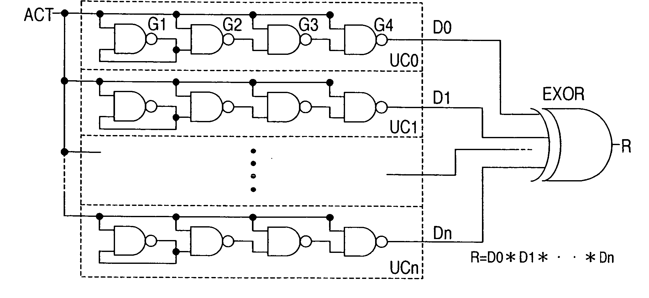
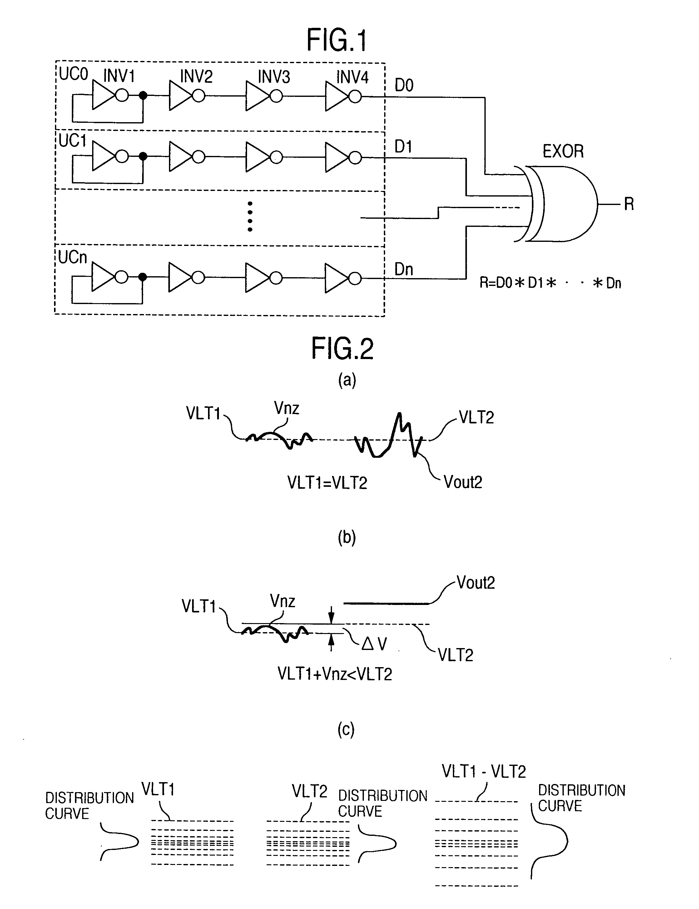
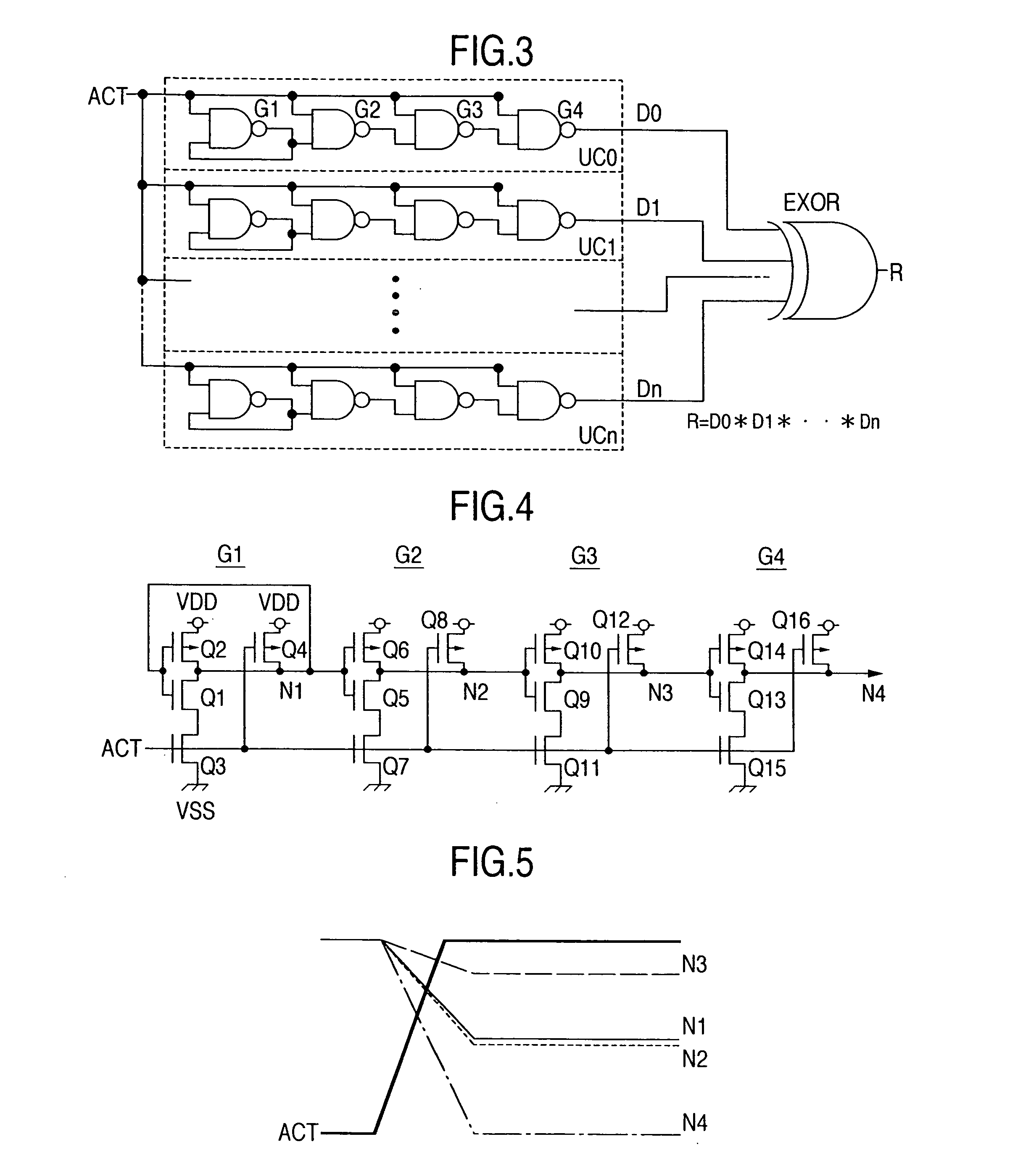
[0042]FIG. 1 shows a circuit diagram of the basic concept of a true random number generating circuit mounted on a semiconductor integrated circuit device according to the present invention. CMOS inverter circuits INV1 to INV4 shown in FIG. 1 are configured so as to have identical characteristic within an actually controllable range according to the design and fabrication of the semiconductor integrated circuit device. The technique for making that a plurality of inverters have identical characteristic will be briefly explained below.

[0043] In a CMOS inverter circuit, it is considered that its characteristic is substantially decided by relative conductance between a P-channel type MOSFET and an N-channel type MOSFET constituting the circuit. In this viewpoint, CMOS inverters of the identical characteristic can be configured by MOSFET having an identical ratio W / L wherein W is the channel width ...


PUM


Abstract

A random number generating method uses: a plurality of unit circuits each having a first and a second logic circuit formed into an identical shape through an identical fabrication process and an amplifier circuit for forming a binary signal by amplifying a noise superposed on the differential voltage of threshold voltages of the first and the second logic circuits; and a signal variation detecting circuit for forming an output signal in response to variation in any of a plurality of binary signals outputted from the plurality of unit circuits, wherein a plurality of binary signals outputted from the signal variation detecting circuit are combined to generate a random number.

Description

TECHNICAL FIELD [0001] The present invention relates to a random number generating method and a semiconductor integrated circuit device and in particular, to a random number generating method appropriate for a semiconductor fabrication technique and a technique which can be effectively used in the semiconductor integrated circuit device. BACKGROUND ART [0002] Recently, networks and IT technique are rapidly spread all over the world, which requires security technique such as the encryption technique and the authentication technique. As one element of these techniques, random numbers are often used. Currently, random number generating circuits based on several types of basic principles have come into practical use. “Toshiba Review” Vol. 58.8 (2003) (first prior art) is an example of ultra-small-size true random number generating circuit for sophisticated information security. Moreover, JP-A-2003-173254 (second prior art) discloses a random number generating circuit using an ambiguous ...

Claims


Application Information

Patent Timeline
IPC IPC(8): G06F7/58
CPCG06F7/588H04L9/06G06F7/58G11C7/06G06F7/57
Inventor MURANAKA, MASAYA
Owner HITACHI ULSI SYST
Why Eureka
Try Eureka