Structure with semiconductor chips embeded therein and method of fabricating same

Active Publication Date: 2007-06-28
PHOENIX PRECISION TECH CORP
View PDF7 Cites 9 Cited by
  • Summary
  • Abstract
  • Description
  • Claims
  • Application Information

AI Technical Summary

Benefits of technology

[0013]In light of the drawbacks of the prior arts described above, a primary objective of the present invention is to provide a structure with semiconducto

Problems solved by technology

Although these techniques can admit high number of leads, when they perform under high frequency or high speed, the conductive paths may be too long, which limit the electrical efficiency.
In addition, since multiple interfaces are required in these conventional techniques, the production cost is increased corresponsively.
Since the shaping machine is relatively large, the preserved space of the carrier board must also be large, thus reducing the usable layout space of the carrier board, and increasing the production cost.
This makes the two opposing surfaces of the package suffer from unbalanced stresses, thereby causing warpage of the carrier board during the process, as well as

Method used


Image

  • Structure with semiconductor chips embeded therein and method of fabricating same
  • Structure with semiconductor chips embeded therein and method of fabricating same
  • Structure with semiconductor chips embeded therein and method of fabricating same

Examples


Example

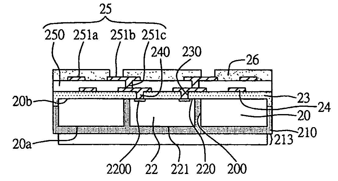
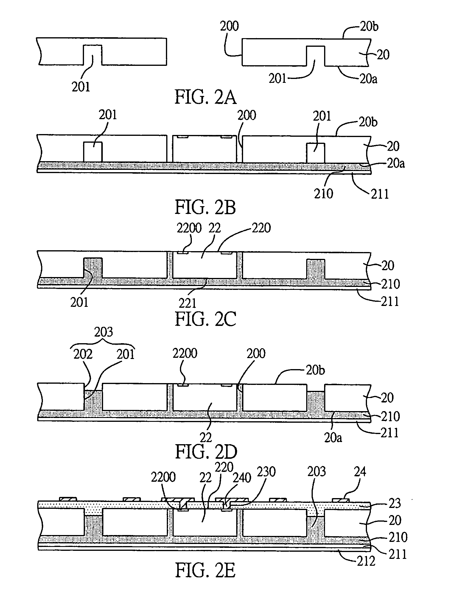
[0027]Preferred embodiments of the present invention will be described in detail below while referring to FIGS. 2A-2I.

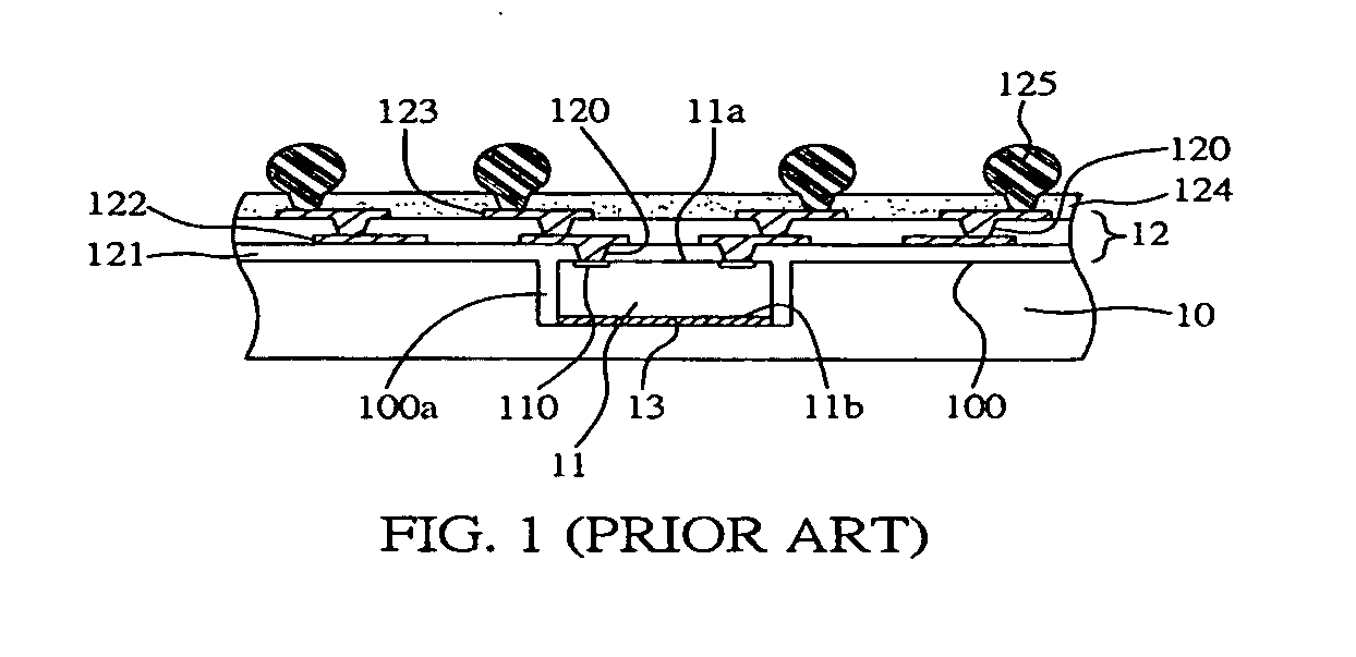
[0028]As shown in FIG. 2A, firstly a carrier board 20 is provided. The carrier board 20 has a first surface 20a and an opposing second surface 20b, therewith forming a plurality of through openings 200 therein, together with first trenches 201 on the first surface 20a thereof surrounding the through openings 200 without penetrating the carrier board 20. The foregoing carrier board 20 can be a heat sink made of metal or an insulating board made of BT resin, RF4 resin, epoxy resin, glass fibre, polyimide, cyanate ester or a circuit board having circuit structure. In the present invention, the first trenches 201 are formed by etching or routing.

[0029]As shown in FIGS. 2B and 2C, a first dielectric layer 210 is provided, and then the first surface 20a of the carrier board 20 is put on the first dielectric layer 210; a semiconductor chip 22 is disposed within each of the ...


PUM


Abstract

An embedded semiconductor chip structure and a method for fabricating the same are proposed. The structure comprises: a carrier board, therewith a plurality of through openings formed in the carrier board, and through trenches surrounding the through openings in the same; a plurality of semiconductor chips received in the through openings of the carrier board. Subsequently, cutting is processed via the through trenches. Thus, the space usage of the circuit board and the layout design are more efficient. Moreover, shaping time is also shortened.

Description

BACKGROUND OF THE INVENTION[0001]1. Field of the Invention[0002]The present invention relates to a structure with semiconductor chips embedded therein and a method of fabricating the same, and more particularly, to a structure with the semiconductor chip embedded and the circuit layer integrated therein, and a method of formation thereof.[0003]2. Background of the Invention[0004]Due to the rapid growth in the electronic industry, electronic devices have gradually been developed towards the directions of multi-function, high speed, and high frequency. In the demand of high integration and miniaturization, semiconductor packages have evolved gradually from a single chip ball grid array (BGA) package or flip chip (FC) package to the types of multi-chip package and module package, such as System in Package (SiP), System Integrated Package (SIP) and System in Board (SiB).[0005]These types of multi-chip package and module package are formed by attaching each semiconductor chip on the carr...

Claims


Application Information

Patent Timeline
IPC IPC(8): H01L23/34
CPCH01L23/5389H01L24/19H01L24/24H01L24/97H01L2221/68377H01L2224/04105H01L2224/20H01L2224/24227H01L2224/97H01L2924/01029H01L2924/01078H01L2924/15153H01L2924/15165H01L2924/1517H01L2924/15311H01L2224/82H01L2924/01033
Inventor ZENG, ZHAO-CHONGHSU, SHIH-PING
Owner PHOENIX PRECISION TECH CORP
Why Eureka
Try Eureka