

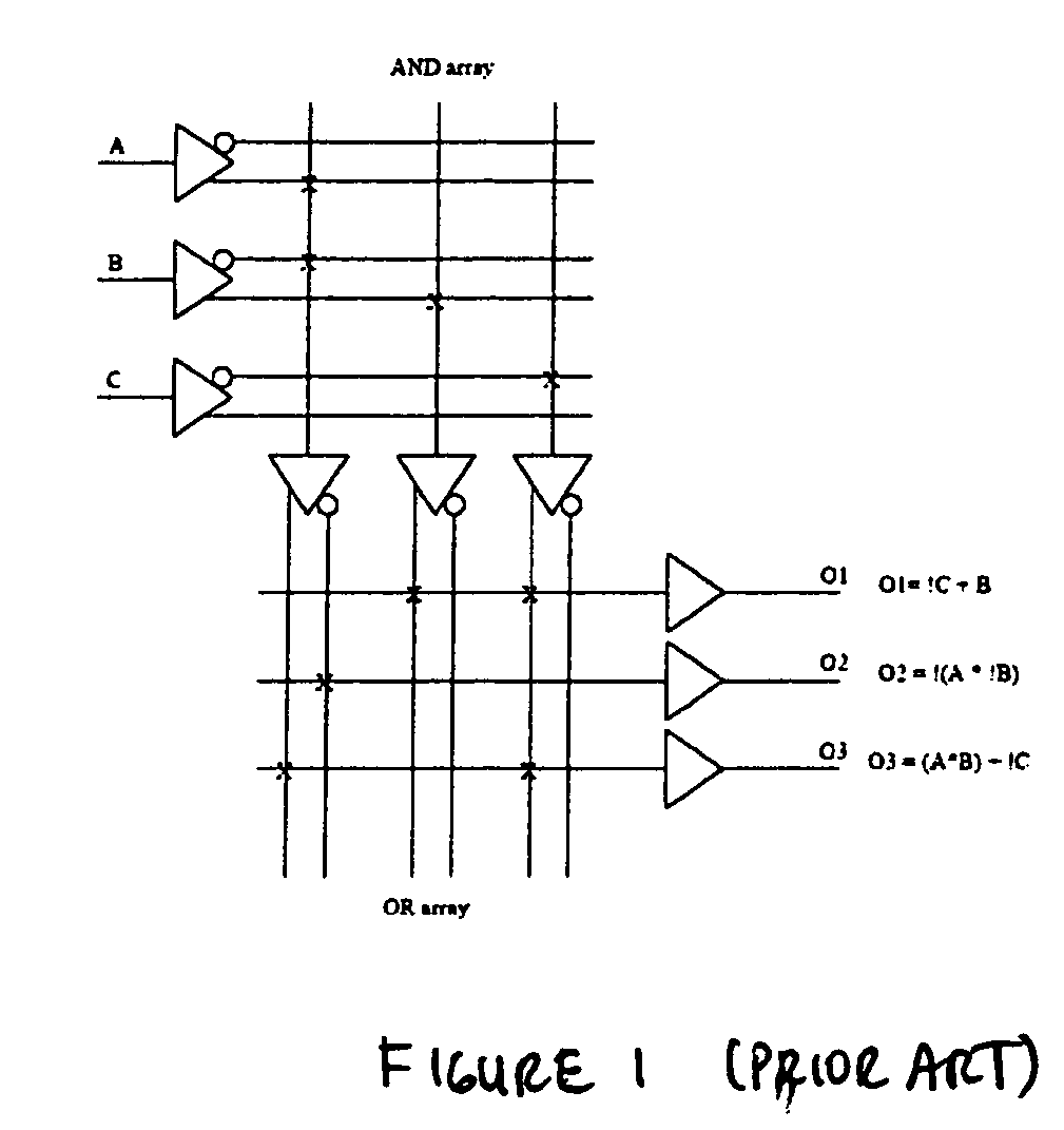
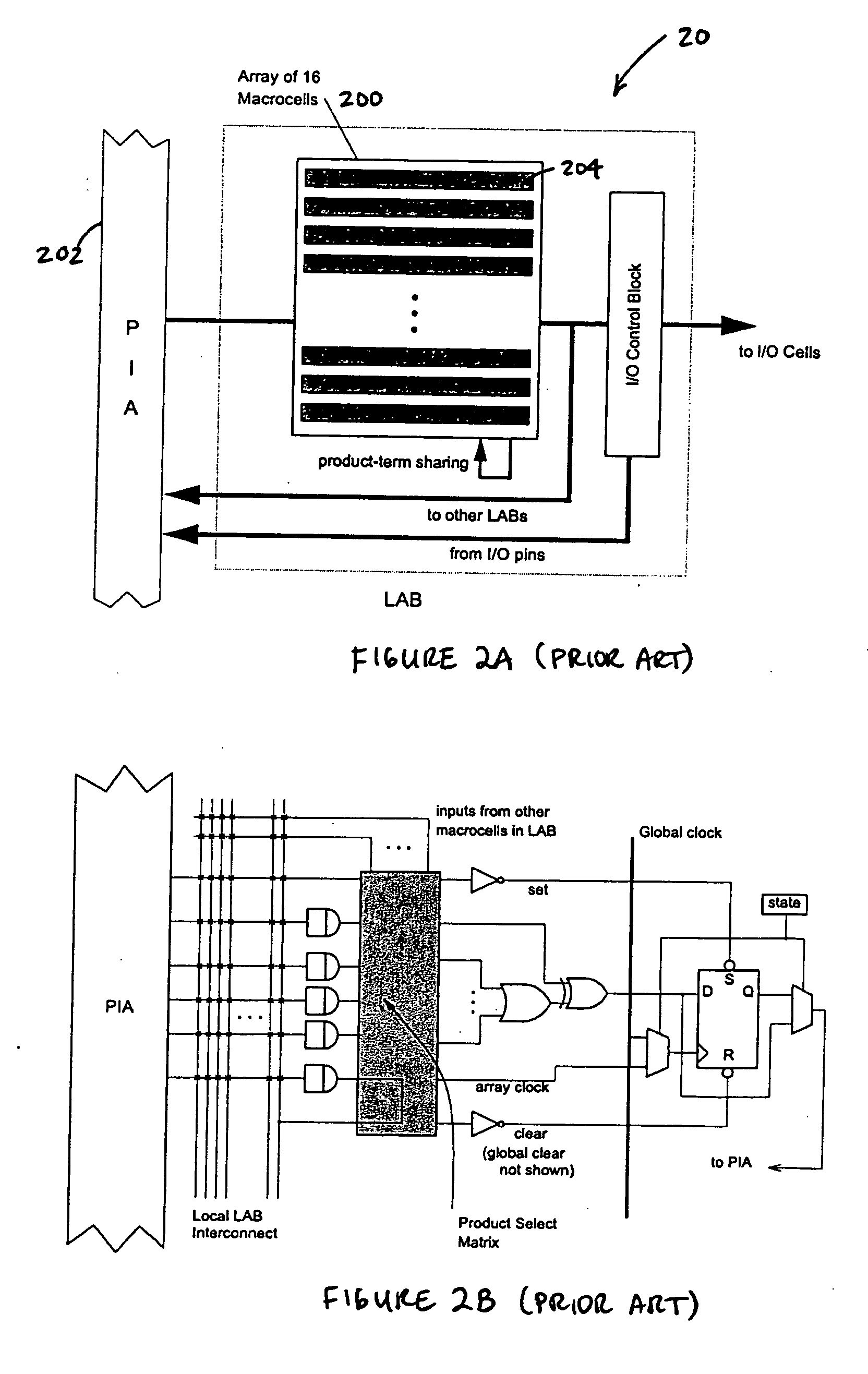
Reconfigurable logic structures
a logic structure and reconfigurable technology, applied in the field of reconfigurable logic structures, can solve the problems of inability to alter functions, limited lifespan of anti-fuse, eeprom/fg and sonos nvm technologies, and early programmable logic device architectures,
- Summary
- Abstract
- Description
- Claims
- Application Information
AI Technical Summary
Benefits of technology
Problems solved by technology
Method used
Image

Examples
Embodiment Construction
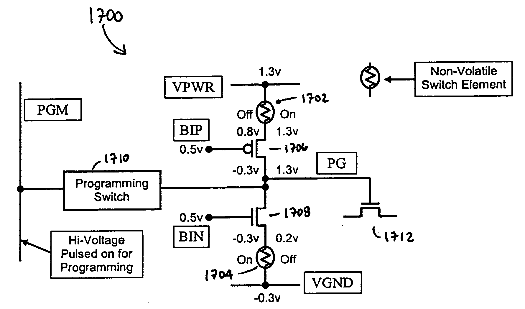
[0057] According to a first aspect of the invention, phase change material devices are used to implement programmable, non-volatile memory elements, which can be used in reconfigurable logic structures. Phase change materials (PCMs) are a class of materials that can change phase from crystalline structures to amorphous structures and vice versa when under different thermal treatments as shown in FIG. 11. When a PCM is heated above its crystallization temperature and cooled down gradually, it solidifies to a crystalline phase and exhibits low electrical resistance. However, when heated above its melting temperature and then cooled down abruptly, the PCM forms an amorphous phase and exhibits high electrical resistance. Accordingly, a PCM may be viewed as a programmable resistor having two distinct electrical resistance values as shown in FIG. 12. PCMs may contain atomic elements from Groups IV, V and VI of the periodic table of elements, such as Ge, As, Se, Te. When formed in an integ...
PUM
 Abstract
Description
Claims
Application Information