Optical functional device and fabrication process of the same

Active Publication Date: 2007-06-28
NEC CORP
View PDF5 Cites 19 Cited by
  • Summary
  • Abstract
  • Description
  • Claims
  • Application Information

AI Technical Summary

Benefits of technology

[0021] Thus, in the optical functional device of the present invention, the functions of optical modulation, optical attenuation and optical switching can be realized by varying amplitude branching ratio K between the branch optical waveguide and ring-type optical waveguide in the optical modulating unit. Amplitude branching ratio K can be easily varied by changing the refractive indexes at the site where th

Problems solved by technology

Since this amplitude branching ratio greatly varies due to the influence of structural errors and other factors, it is difficult to fabricate and adjust the device so as to satisfy the desirable characteristics.
However, the electroabsorption modulator proposed by Ishizuka et al. suffers from difficulties in reducing cost from the viewpoint of the used wafer material and fabrication cost.
However, the device configuration is to perform no more than conversion of the change in refractive index caused by application of an electric field to the vicinity of a PN junction into light intensity by use of a simple Mach-Zehnder interference optical system, and a device size equal to or greater than 1 cm is needed.
So, there is not only a limit to cost reduction from the viewpoint of the yield obtained fr

Method used


Image

  • Optical functional device and fabrication process of the same
  • Optical functional device and fabrication process of the same
  • Optical functional device and fabrication process of the same

Examples


first embodiment

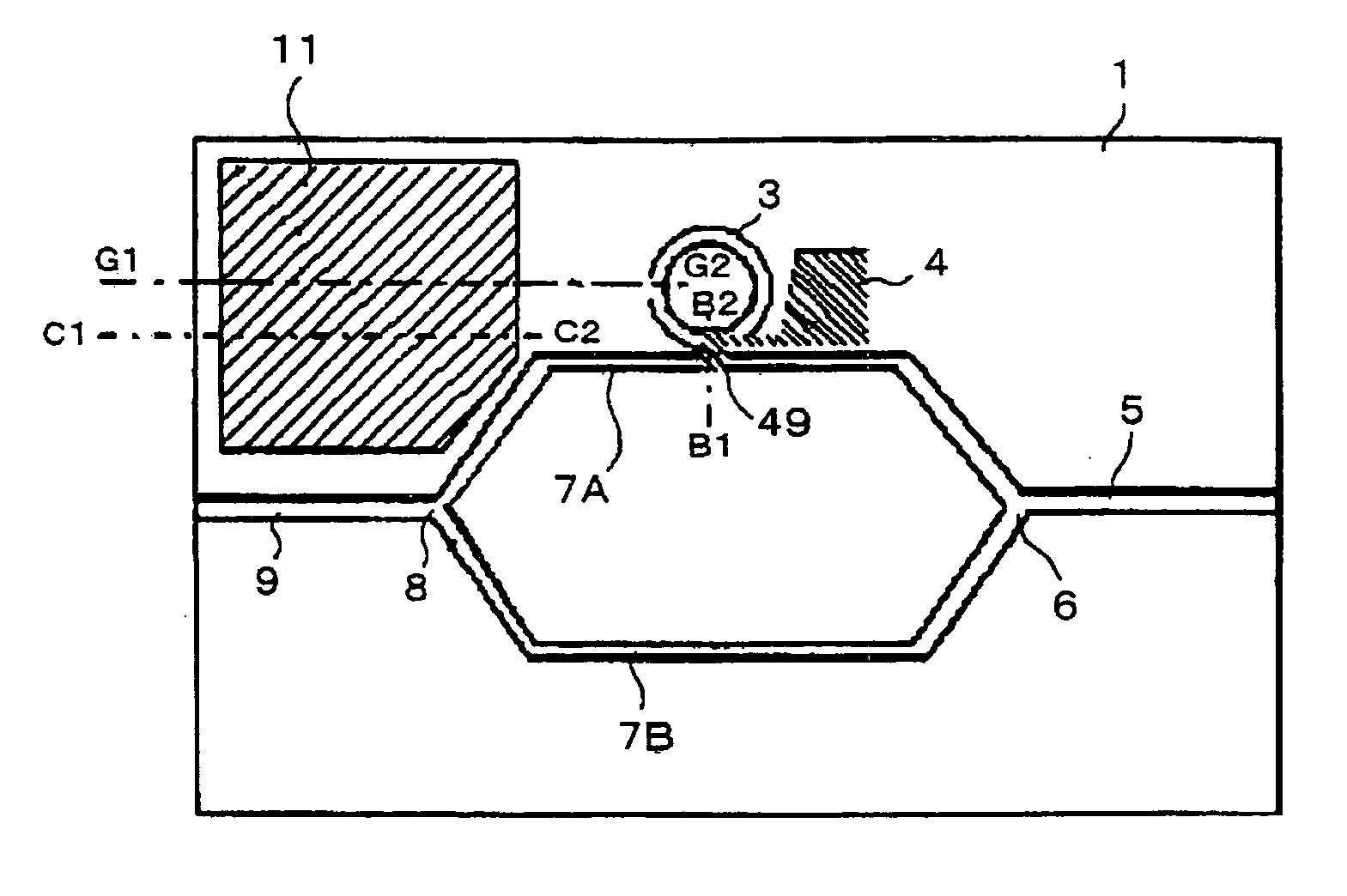
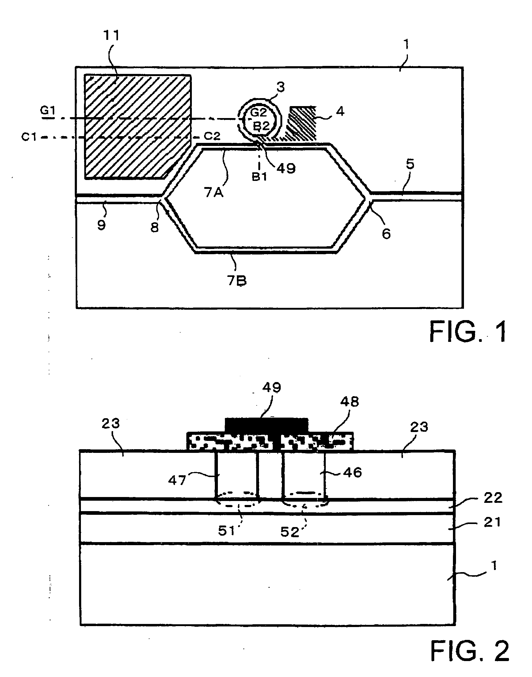
[0040]FIG. 1 shows a configuration of an optical functional device according to the first embodiment of the present invention. Here, the optical functional device is given as a Mach-Zehnder type optical modulator.

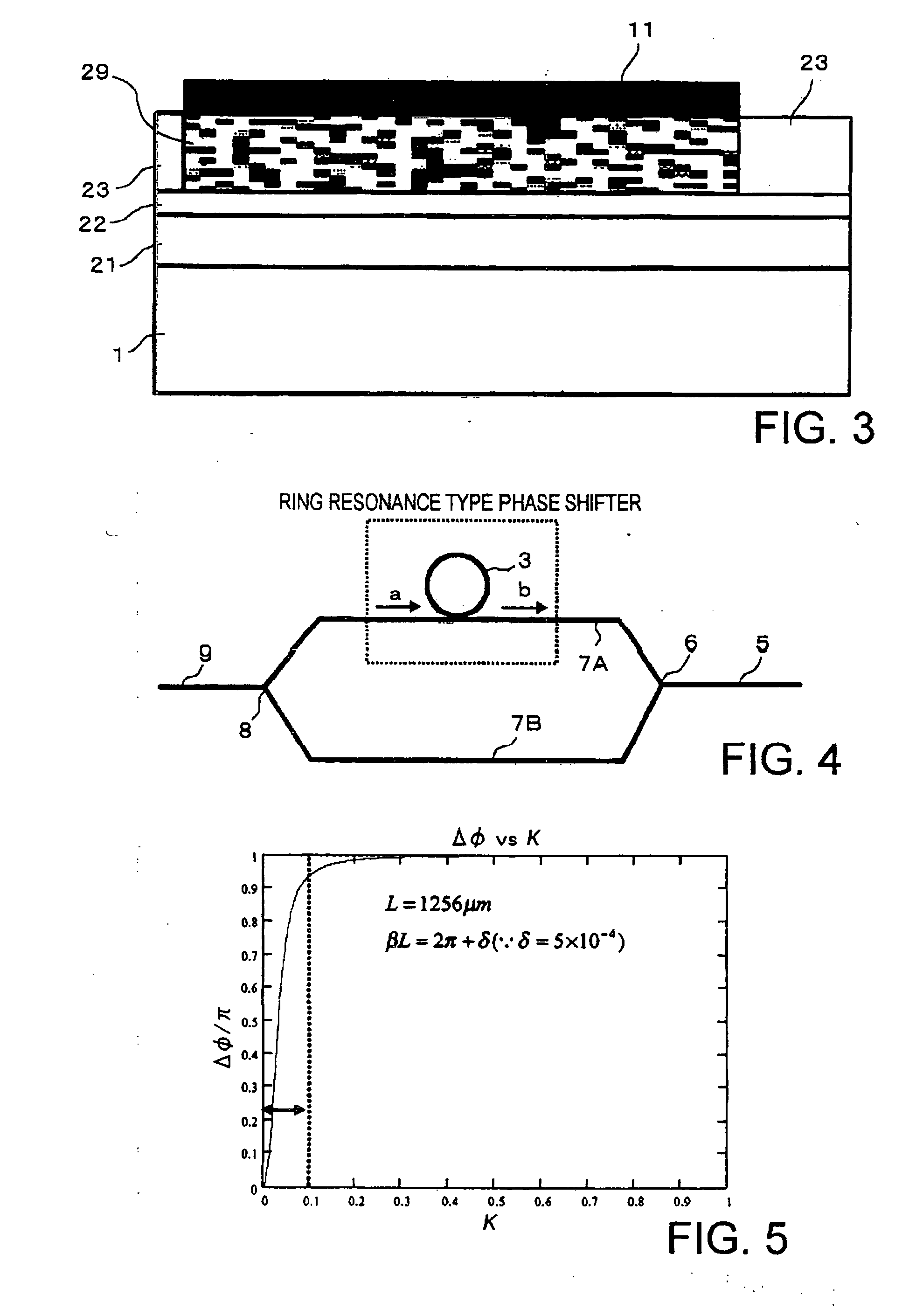
[0041] Formed on one planar surface on top of silicon substrate 1 are input optical waveguide 9 which receives a light wave signal from its one end, splitter 8 connected to the other end of input optical waveguide 9, a pair of branch optical waveguides 7A, 7B, combiner 6 which combines light wave signals having passed through the two branch optical waveguides 7A, 7B, output optical waveguide 5 for outputting the light wave signal that was combined at combiner 6, and ring-type optical waveguide 3 to be mode-coupled with one branch optical waveguide 7A. Ring-type optical waveguide is arranged close to this branch optical waveguide 7A. Though in the figure, branch optical waveguides 7A, 7B are provided as linear configurations, these may be formed in curved shapes. Splitter 8...

second embodiment

[0059] Next, as the second embodiment of the present invention, a Mach-Zehnder type optical attenuator that will operate with low power consumption will be described. FIG. 7 shows an optical attenuator according to the second embodiment. FIG. 8 shows the section cut along line D1-D2 in FIG. 7. In FIGS. 7 and 8, the same components as those shown in FIGS. 1 to 3 are allotted with the same reference numerals.

[0060] Similarly to the optical modulator of the first embodiment, this optical attenuator uses a ring resonance type phase shifter made up of ring-type optical waveguide 3 and branch optical waveguide 7A. Amplitude branching ratio K between ring-type optical waveguide 3 and branch optical waveguide 7A is controlled so as to vary the intensity of the light wave signal emitted from output optical waveguide 5. Here in this embodiment, heater 65 is arranged at the site where ring-type optical waveguide 3 and branch optical waveguide 7A are mode-coupled, and a change in temperature i...

third embodiment

[0067] Next, an optical modulator according to the third embodiment of the present invention will be described. FIG. 9 shows an optical modulator of the third embodiment. This optical waveguide has a similar configuration to the optical modulator of the first embodiment, and FIG. 9 corresponds to the section cut along line B1-B2 in FIG. 1. However, in the optical modulator of the present embodiment, in order to make amplitude branching ratio K between branch optical waveguide 7A and ring-type optical waveguide 3 variable, EO effect layer (i.e., electro-optic effect device) 130 made up of a material having electro-optic effect is arranged in the area between the cores of optical waveguides 3, 7A in the area where branch optical waveguide 7A and ring-type optical waveguide 3 are mode-coupled. Since in this optical modulator, the magnitude of the EO effect varies in accordance with the voltage applied to EO effect layer 130, it is possible to vary the coupled state between the two opti...


PUM


Abstract

Arranged for at least one of a pair of branch optical waveguides in a Mach-Zehnder type interference optical system is a ring resonance type phase shifter for modulating a light wave signal propagating through the branch optical waveguide. The ring resonance type phase shifter includes a ring-type optical waveguide arranged so as to be mode-coupled with the corresponding branch optical waveguide, and is configured so that amplitude branching ratio K between the corresponding branch optical waveguide and the ring-type optical waveguide can be varied with a change in refractive index or the like, accompanied by voltage application to a pn junction, for example. As amplitude branching ratio K is varied, the phase difference between the light wave signals propagating through the paired optical waveguides varies, to thereby control the intensity of the light wave signal output from the interference optical system.

Description

BACKGROUND OF THE INVENTION [0001] 1. Field of the Invention [0002] The present invention relates to an optical functional device for use in optical communication, optical information processing, optical interconnections and the like, and in particular relating to an optical functional device such as an optical modulator for converting electric signals into optical signals, variable optical attenuator, and a driving method and a fabrication process of such optical functional devices. [0003] 2. Description of the Related Art [0004] Optical functional devices or photonic devices, represented by an optical modulator which converts an electric signal as the modulation signal into an optical signal, an optical attenuator which attenuates an optical signal in accordance with an electric signal that represents the amount of attenuation, are key components that play markedly important roles in association with rapid increase in communication traffic on the recent optical communication marke...

Claims


Application Information

Patent Timeline
IPC IPC(8): G02F1/295
CPCG02F1/0147G02F1/025G02F1/035G02F1/2257G02F2001/0152G02F2001/212G02F2202/10G02F2202/20G02F2203/055G02F2203/15G02F2203/50G02F1/0152G02F1/212
Inventor ISHIZAKA, MASASHIGE
Owner NEC CORP
Why Eureka
Try Eureka