Method for fabricating semiconductor device and method for fabricating magnetic head

a semiconductor device and magnetic head technology, applied in the field of semiconductor device fabrication and method for fabricating magnetic head, can solve the problems of unignorable operation characteristics and affecting the generation rate of conduction defects of interconnection layers, and affecting the reliability of semiconductor devices, etc., to achieve good stress-migration resistance, reduce the generation rate of conduction defects of interconnection layers, and high reliability

Inactive Publication Date: 2007-06-28
FUJITSU LTD
View PDF21 Cites 6 Cited by
  • Summary
  • Abstract
  • Description
  • Claims
  • Application Information

AI Technical Summary

Benefits of technology

[0011] An object of the present invention is to provide a method for fabricating a semiconductor device which suppresses the generation of voids in the interconnection layers in high temperature environments to thereby suppress the conduction defects of the interconnection layers, and improves the reliability of the semiconductor device.
[0012] Another object of the present invention is to provide a method for fabricating a magnetic head which suppresses the generation of voids in the interconnection layers in high temperature environments to thereby suppress the conduction defects of the interconnection layers, and improves the reliability of the magnetic head.
[0015] The method for fabricating a semiconductor device according to the present invention comprises the steps of: forming an opening in an insulation film; forming an interconnection layer of Cu as a main material in the opening; and performing nitrogen-two-fluid processing of concurrently spraying pure water with ammonia and hydrogen solved in and nitrogen gas on a surface of the interconnection layer buried in the opening, whereby the migration of the Cu atoms of the interconnection layer in a high temperature environment is suppressed, and the generation rate of conduction defects of the interconnection layer can be decreased. Thus, the semiconductor devices having multilayer interconnection layers of good stress-migration resistance and high reliability can be provided.
[0016] The method for fabricating a magnetic head according to the present invention comprises the steps of: forming an opening of a pattern of a coil in an insulation film; forming an interconnection layer formed of Cu as a main material and forming a coil in the opening; and performing nitrogen-two-fluid processing of concurrently spraying pure water with ammonia and hydrogen solved in and nitrogen gas on a surface of the interconnection layer buried in the opening, whereby the migration of the Cu atoms of the interconnection layer in a high temperature environment is suppressed, and the generation rate of conduction defects of the interconnection layer forming the coil can be decreased. Thus, the magnetic heads having multilayer interconnection layers of high reliability can be provided.

Problems solved by technology

Conventionally, the interconnection layers have been formed by depositing interconnection materials and patterning the deposited interconnection materials using lithography and dry etching, but technical limitations in this process commences to arise as the generation has advanced.
It has been conventionally known that when the multilayer interconnection structure is exposed to high temperature environment due to such temperature rise in operation and the processes following the formation of the multilayer interconnection structure, etc., Cu atoms in the interconnection layers and pores formed in the interconnection layers migrate, forming large voids in the interconnection layers, and these voids causes conduction defects of the interconnection layers.
However, in the generation where widths of the interconnection layers were 0.5 μm or less, the influences of the interconnection resistance increase due to voids generated in the interconnection layers on the operation characteristics and reliability of semiconductor devices become unignorable.
So far, sufficient countermeasures to the conduction defects of the interconnection layers due to the voids caused by heat have not been made.

Method used


Image

  • Method for fabricating semiconductor device and method for fabricating magnetic head
  • Method for fabricating semiconductor device and method for fabricating magnetic head
  • Method for fabricating semiconductor device and method for fabricating magnetic head

Examples


first embodiment

A FIRST EMBODIMENT

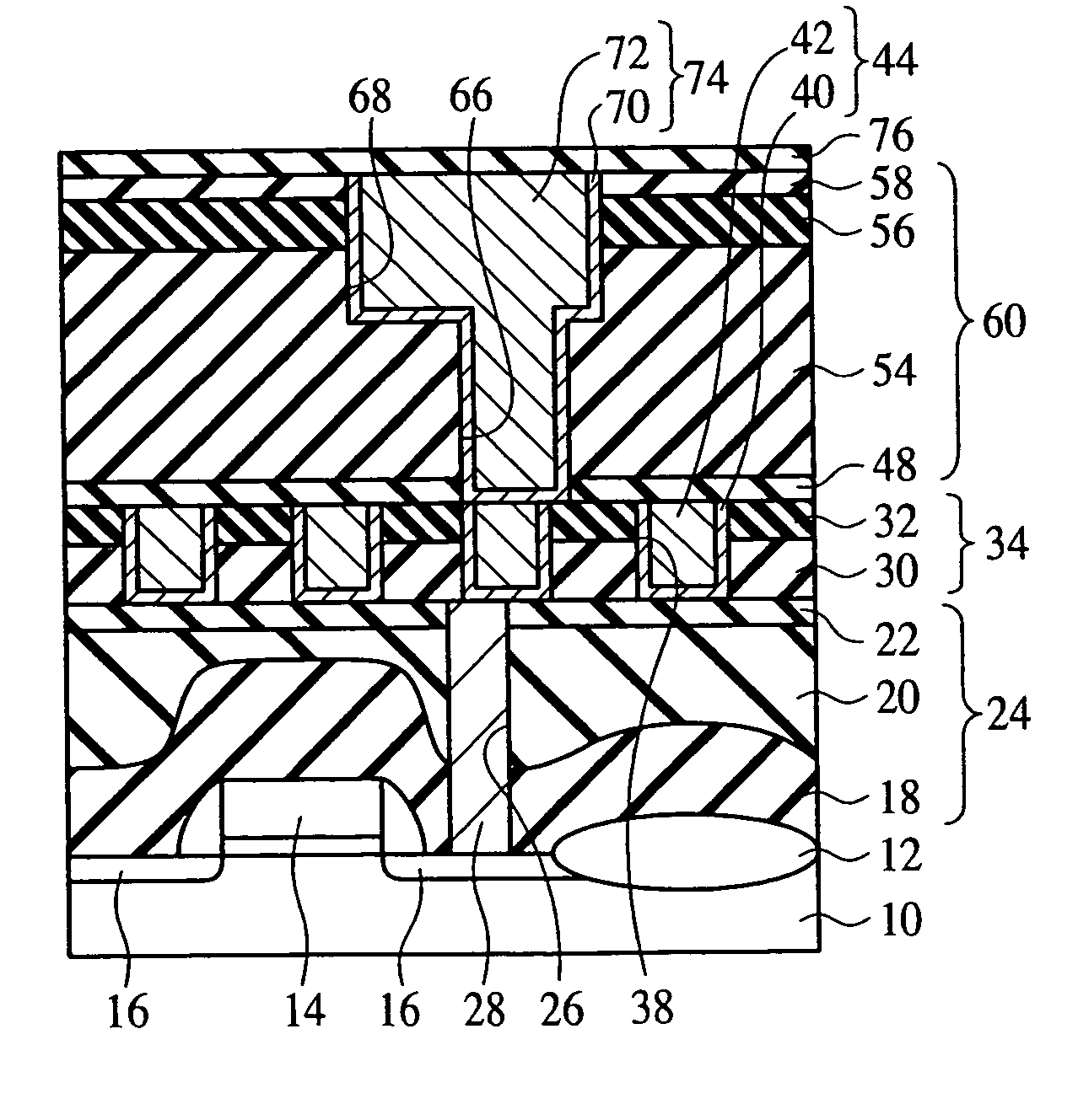
[0063] The method for fabricating a semiconductor device according to a first embodiment will be explained with reference to FIGS. 4A-4D, 5A-5C, 6A-6C, 7A-7B, 8A-8B, 9A-9B, 10A-10B and 11A-11B. FIGS. 4A-4D, 5A-5C, 6A-6C, 7A-7B, 8A-8B, 9A-9B, 10A-10B and 11A-11B are sectional views of the semiconductor device in the steps of the method for fabricating the same according to a first embodiment of the present invention, which show the method.

[0064] First, in the same way as in, e.g., the usual MOS transistor fabricating method, a MOS transistor including a gate electrode 14 and a source / drain diffused layers 16 is formed on a silicon substrate 10 with a device isolation film 12 formed on (see FIG. 4A). Various semiconductor devices other than MOS transistors can be fabricated on the semiconductor substrate 10.

[0065] Then, a silicon nitride film 18 of, e.g., a 0.1 μm-thickness is formed by, e.g., CVD (Chemical Vapor Deposition) on the silicon substrate 10 with the MOS...

second embodiment

A SECOND EMBODIMENT

[0119] The method for fabricating a magnetic head according to a second embodiment of the present invention will be explained with reference to FIGS. 12, 13A-13C, 14A-14C and 15A-15C. FIG. 12 is a perspective of a magnetic head, which illustrates a structure thereof. FIGS. 13A-13C, 14A-14C and 15A-15C are sectional views of the magnetic head in the steps of the method for fabricating the same according to the present embodiment, which show the method.

[0120]FIG. 12 illustrates the structure of the induction type thin-film magnetic head for hard discs. FIGS. 13A-13C, 14A-14C and 15A-15C illustrate the steps forming the first layer and the second layer of the coil of the induction type thin-film magnetic head illustrated in FIG. 12. In FIGS. 13A-13C, 14A-14C and 15A-15C, the members except the coil are suitably omitted. In the following description, the reproduction head will be omitted, and only the induction type thin-film magnet head will be explained.

[0121] Fir...


PUM


Abstract

The method comprises the step of forming an interconnection trench 38 in an inter-layer insulation film 34, the step of forming an interconnection layer 44 of Cu as the main material in the interconnection trench 38, and the step of performing nitrogen-two-fluid processing of concurrently spraying pure water with ammonia and hydrogen solved in and nitrogen gas on the surface of the interconnection layer44 buried in the interconnection trench 38.

Description

CROSS-REFERENCE TO RELATED APPLICATIONS [0001] This application is based upon and claims the benefit of priority from the prior Japanese Patent Application No. 2005-379531, filed on Dec. 28, 2005, the entire contents of which are incorporated herein by reference. BACKGROUND OF THE INVENTION [0002] The present invention relates to a method for fabricating a semiconductor device having an interconnection structure using copper as a main material of the interconnection layer, and a method for fabricating a magnetic head having an interconnection structure using copper as a main material of the interconnection layer. [0003] As semiconductor devices have been larger scaled and higher integrated, the design rule of the interconnections has been reduced with the generations. Conventionally, the interconnection layers have been formed by depositing interconnection materials and patterning the deposited interconnection materials using lithography and dry etching, but technical limitations in...

Claims


Application Information

Patent Timeline
Patent Type & Authority Applications(United States)
IPC IPC(8): H01L21/4763
CPCG11B5/3163H01L21/02074H01L21/321H01L21/76877H01L21/76886H01L21/3205
Inventor ITANI, TSUKASASASAKI, MAKOTOTAKIGAWA, YUKIO
Owner FUJITSU LTD
Why Eureka
Try Eureka