Substrate for photoelectric conversion device, photoelectric conversion device, and stacked photoelectric conversion device

a photoelectric conversion and substrate technology, applied in the direction of basic electric elements, electrical apparatus, semiconductor devices, etc., can solve the problems of global warming phenomenon, depletion of future resources, lack of raw materials, etc., and achieve the effect of enhancing the photoelectric conversion efficiency of the photoelectric conversion device, enhancing the transmittance of the first transparent conductive layer, and reducing the cost of raw materials

Inactive Publication Date: 2007-07-05
SHARP KK
View PDF8 Cites 205 Cited by
  • Summary
  • Abstract
  • Description
  • Claims
  • Application Information

AI Technical Summary

Benefits of technology

[0023] In accordance with the first present invention, the first transparent conductive layer has at least an opening portion and therefore light can pass through the opening portion at high transmittance. Therefore, in accordance with the first present invention, the transmittance of the first transparent conductive layer can be substantially enhanced even when the film thickness of the first transparent conductive layer is thick. And, when a photoelectric conversion device is fabricated using the substrate for a photoelectric conversion device of the first present invention, the photoelectric conversion efficiency of the photoelectric conversion device can be enhanced.
[0024] And, the first transparent conductive layer can have a high haze index by having a texture structure on its surface. Therefore, in this case, it is possible to attain both high transmittance and a high haze index. And, when a photoelectric conversion device is fabricated using this substrate for a photoelectric conversion device, the photoelectric conversion efficiency of the photoelectric conversion device can be further enhanced.
[0025] And, by further providing the substrate for a photoelectric conversion device of the first present invention with a second transparent conductive layer covering the opening portion of the first transparent conductive layer on the first transparent conductive layer, a sheet resistance of the overall transparent conductive layer can be reduced. And, the second transparent conductive layer can be formed so as to have a thinner film thickness than that of the first transparent conductive layer, and a reduction in the transmittance of the overall transparent conductive layer can be made small. Accordingly, in this case, it is possible to achieve high transmittance, a high haze index and a low sheet resistance simultaneously. And, when a photoelectric conversion device is fabricated using this substrate for a photoelectric conversion device, the photoelectric conversion efficiency of the photoelectric conversion device can be further enhanced. (Effects of Second Present Invention)
[0026] Either one of a pair of photoelectric conversion layers, between which the intermediate layer is sandwiched, becomes a top cell, and the other becomes a bottom cell.
[0027] In accordance with the second present invention, since the intermediate layer has at least an opening portion, light having reached the intermediate layer can pass through the intermediate layer at high transmittance. Consequently, the quantity of incident light entering the bottom cell increases.
[0028] In accordance with the second present invention, the quantity of incident light entering the bottom cell can be controlled by controlling a size, a density or the like of the opening portion formed in the intermediate layer. Therefore, it is possible to form the opening portion in such a way that the short circuit current density of the bottom cell becomes equal to that of the top cell and to obtain a high-efficiency stacked photoelectric conversion device can be obtained.

Problems solved by technology

On fossil fuels such as petroleum and the like, there are a fear of future resource depletion and a problem of carbon dioxide emission causing a global warming phenomenon.
But, recently, there are problems that raw materials are lacking because of rapidly increasing production of the bulk solar cell and cost reduction is difficult.
First, light absorption in the above transparent conductive layer is low, that is, the transparent conductive layer has high transmittance.
However, when a substrate having a surface texture structure in which the level difference between projections and depressions of a texture structure is large and the pitch of projections and depressions of a texture structure is small is used, there are problems that mechanical or electrical defects resulting from the texture structure tends to occur and these defects causes the reduction in the open circuit voltage of the photoelectric conversion device or the reduction in the yield.
Therefore, it is thought that this causes variations in the performance of the photoelectric conversion device to be larger.

Method used


Image

  • Substrate for photoelectric conversion device, photoelectric conversion device, and stacked photoelectric conversion device
  • Substrate for photoelectric conversion device, photoelectric conversion device, and stacked photoelectric conversion device
  • Substrate for photoelectric conversion device, photoelectric conversion device, and stacked photoelectric conversion device

Examples


first embodiment

1. First Embodiment

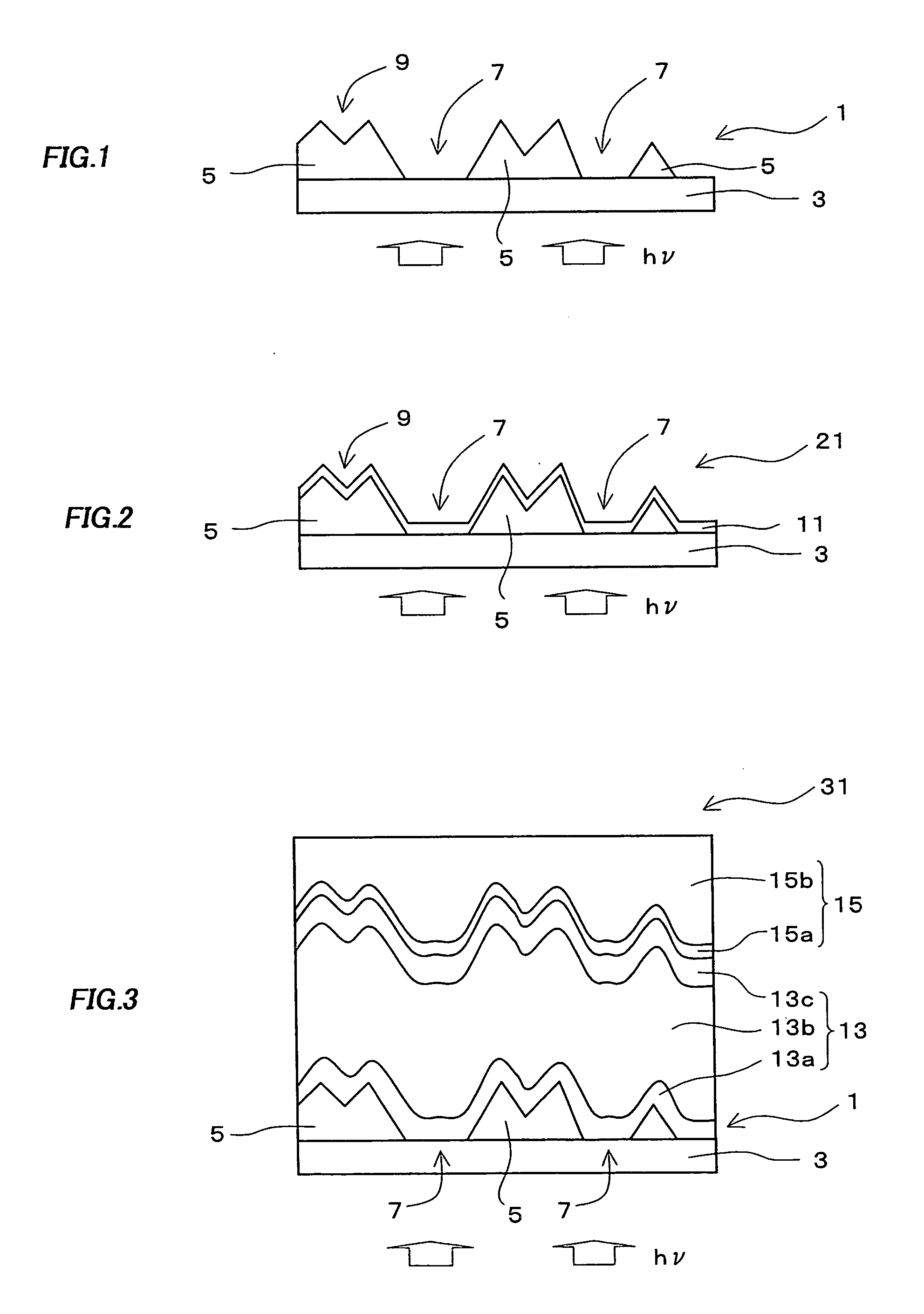
[0093] A substrate for a photoelectric conversion device of the first embodiment of the first present invention includes a first transparent conductive layer formed on at least a part of the surface region of a substrate and the first transparent conductive layer has at least an opening portion exposing the substrate.

1-1. Substrate

[0094] In a photoelectric conversion device having a structure of a superstrate type, a transparent substrate is employed as the above substrate, but in a photoelectric conversion device having a structure of a substrate type, a non-transparent substrate such as stainless steel or the like may be used as the above substrate. Hereinafter, a substrate for a photoelectric conversion device having a structure of a superstrate type will be described, but these descriptions can also be applied to the case where the photoelectric conversion device has a structure of a substrate type. As a material of the transparent substrate, glass, resin h...

second embodiment

2. Second Embodiment

[0121] In a photoelectric conversion device of the second embodiment of the first present invention, a photoelectric conversion layer and a backside electrode layer are stacked in this order on the substrate for a photoelectric conversion device in the first embodiment. Hereinafter, a photoelectric conversion device having a structure of a superstrate type will be described, but these descriptions can also be applied to the case where the photoelectric conversion device has a structure of a substrate type.

[0122] Since the photoelectric conversion layer is formed on the substrate of the first embodiment, the quantity of light entering the photoelectric conversion layer can be enhanced and the short circuit current density of a photoelectric conversion device can be improved.

2-1. Photoelectric Conversion Layer

[0123] The photoelectric conversion layer is formed on the substrate for a photoelectric conversion device of the first embodiment. Generally, a p-n juncti...

third embodiment

3. Third Embodiment

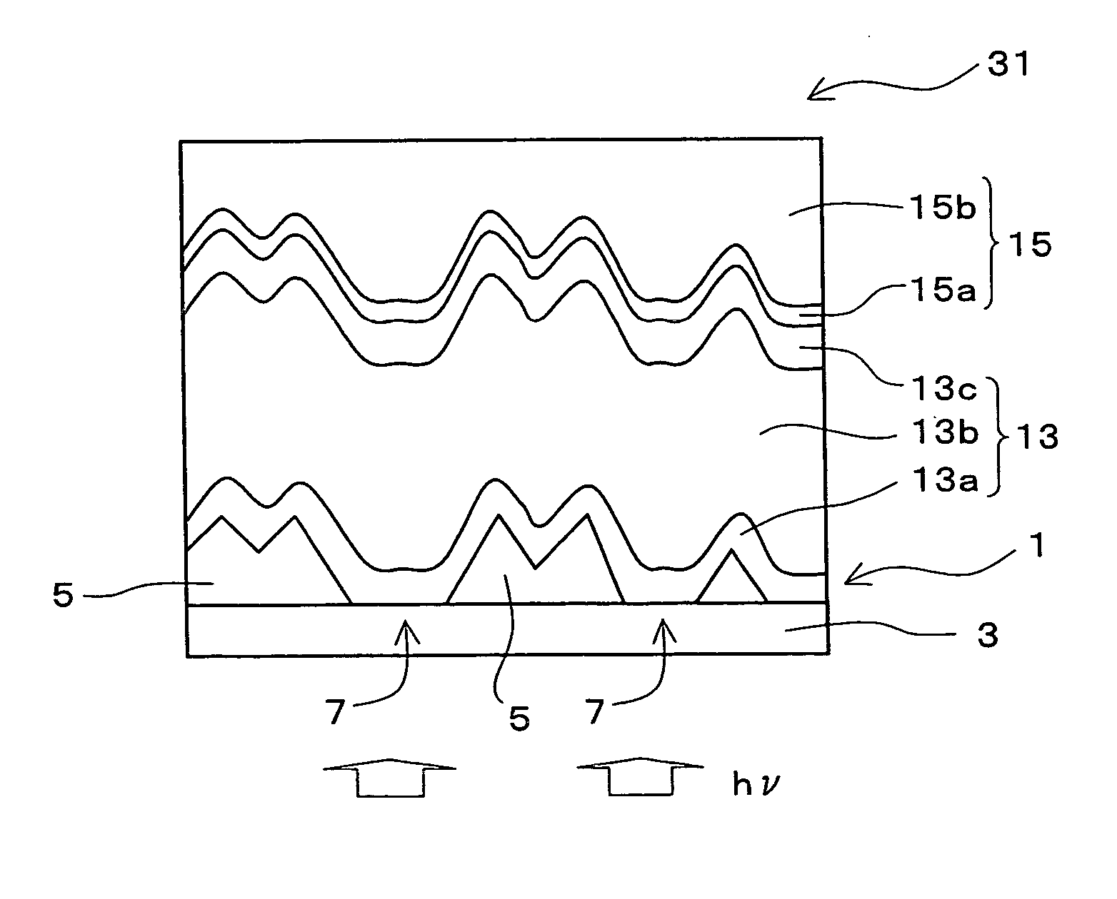
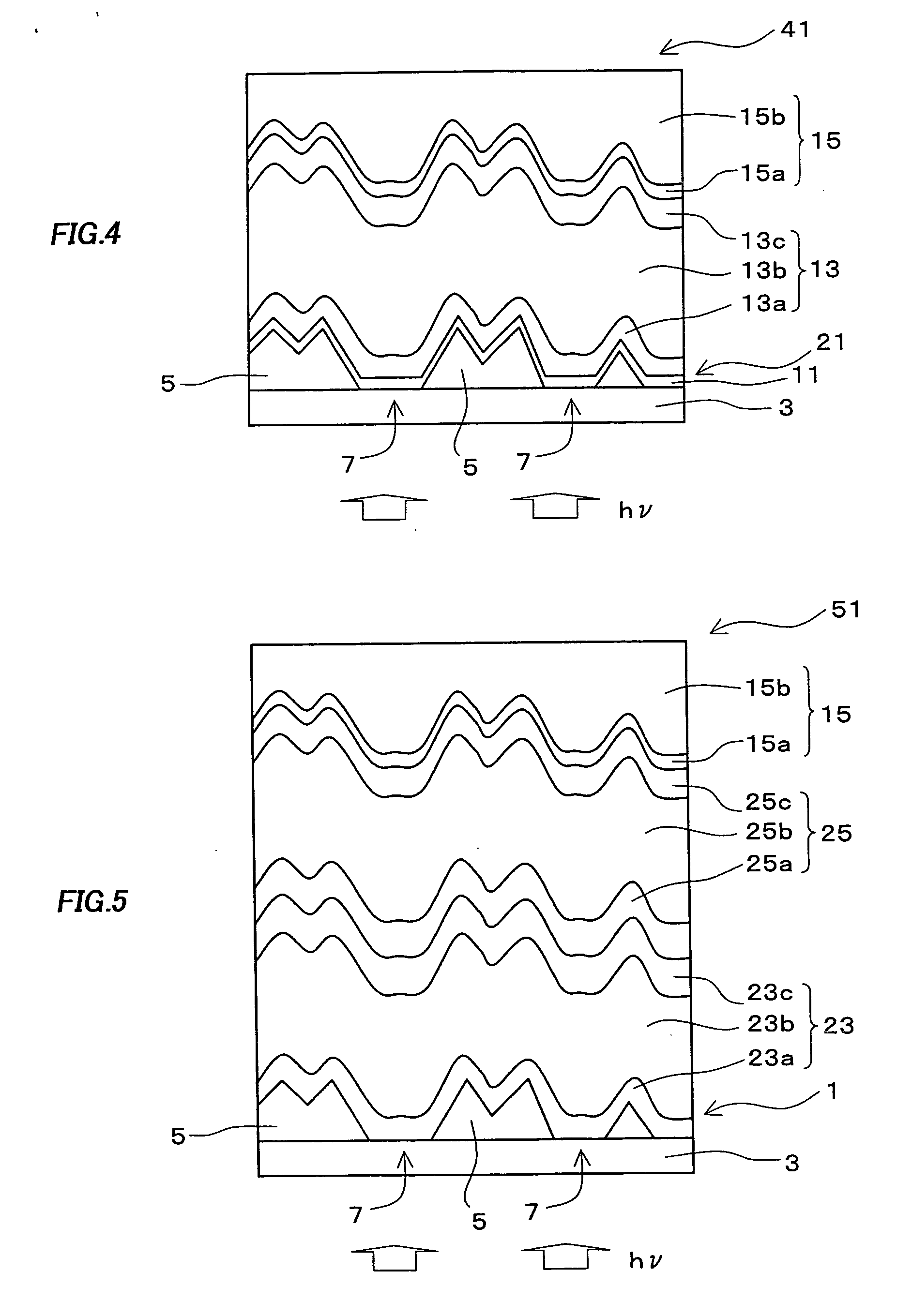
[0132] In a stacked photoelectric conversion device of the third embodiment of the first present invention, a plurality of photoelectric conversion layers and a backside electrode layer are stacked in this order on the substrate for a photoelectric conversion device in the first embodiment. Hereinafter, a stacked photoelectric conversion device having a structure of a superstrate type will be described, but these descriptions can also be applied to the case where the stacked photoelectric conversion device has a structure of a substrate type.

[0133] Since the stacked photoelectric conversion device of the present embodiment has a plurality of photoelectric conversion layers, it can receive the split light spectrum in each photoelectric conversion layer by splitting a wide light spectrum region and make effective use of light. And, since the open circuit voltage is sum of the electromotive forces in the respective photoelectric conversion layers, the open circuit v...


PUM


Abstract

A substrate 1 for a photoelectric conversion device includes a first transparent conductive layer 5 formed on at least a part of the surface region of a transparent substrate 3, the first transparent conductive layer 5 having at least an opening portion 7 exposing the substrate 3.

Description

TECHNICAL FIELD [0001] The present invention relates to a substrate for a photoelectric conversion device, a photoelectric conversion device, and a stacked photoelectric conversion device, which can attain a high photocurrent and high photoelectric conversion efficiency. BACKGROUND ART [0002] On fossil fuels such as petroleum and the like, there are a fear of future resource depletion and a problem of carbon dioxide emission causing a global warming phenomenon. In recent years, photo voltaic systems become widespread particularly by growing environmental concerns and the cost-reduction of systems and are expected as alternative energy sources of fossil fuels such as petroleum and the like. [0003] Common solar cells are classified into a bulk solar cell and a thin film solar cell. The bulk solar cell is made using a semiconductor of a bulk crystal such as monocrystalline silicon or polycrystalline silicon, or a gallium arsenide compound solar cell or the like, and in many of the sola...

Claims


Application Information

Patent Timeline
Patent Type & Authority Applications(United States)
IPC IPC(8): H01L31/00H01L31/0224H01L31/06H01L31/076H01L31/077
CPCH01L31/022466H01L31/0236Y02E10/548H01L31/1884H01L31/076H01L31/022483H01L31/02363H01L31/02366Y02E10/547
Inventor NASUNO, YOSHIYUKIKOHAMA, NORIYOSHINISHIMURA, KAZUHIKOHAYAKAWA, TAKASHI
Owner SHARP KK
Why Eureka
Try Eureka