Method for surface imprinted films with carbon nanotubes

a technology of carbon nanotubes and imprinting films, applied in nanoinformatics, organic semiconductor devices, manufacturing tools, etc., can solve the problems of limiting the application of nil to flexible plastic substrates envisioned, the relative geometry of nanoscale components is limited, and the process is difficult to achieve the effect of achieving the effect of nil application

Active Publication Date: 2007-07-05
THE UNITED STATES OF AMERICA AS REPRESENTED BY THE SECRETARY OF THE NAVY
View PDF4 Cites 22 Cited by
  • Summary
  • Abstract
  • Description
  • Claims
  • Application Information

AI Technical Summary

Benefits of technology

[0014] The present invention relates to methods of making films surface imprinted with nanometer-sized particles to produce micro- and / or nano-structured electron and hole collecting interfaces. Embodiments of the method of making these films include: providing at least one transparent substrate, providing at least one photoabsorbing conjugated polymer, providing a sufficient amount of nanometer-sized particles to produce a charge separation interface, providing at least one transparent polymerizable layer including a sol-gel or monomer, embedding the nanometer-sized particles in the conjugated polymer, applying the polymerizable layer on a first substrate to form a charge transport film layer, applying the conjugated polymer / nanometer-sized particle mixture on a second substrate to form a nanometer-sized particles bearing surface film layer, wherein the nanometer-sized particles form a stamp surface, imprinting the stamp surface into the surface of the polymerizable film layer to produce micro- and / or nano-structured electron and hole collecting interfaces, polymerizing the polymerizable film layer to promote shrinkage to form a conformal gap between the stamp surface and the surface of the polymerizable film layer, and filling the gap with at least one photoabsorbing material to promote the generation of photoexcited electrons and transport to the charge separation interface.

Problems solved by technology

The most successful patterning technique used over the past several decades has been photolithography, although developments in this technique have pushed feature resolution to the 40 nm range and have come at the expense of increasingly complex and costly fabrication equipment.
This heating process limits the application of NIL to flexible plastic substrates envisioned for a broad range of emerging applications, since many of these plastics deform at elevated temperatures.
This technique is limited in that it requires a elastomeric stamp and thus the degree to which the relative geometry of nanoscale components are in registry is limited by the ability to position the stamp from layer to layer.

Method used


Image

  • Method for surface imprinted films with carbon nanotubes
  • Method for surface imprinted films with carbon nanotubes

Examples


examples

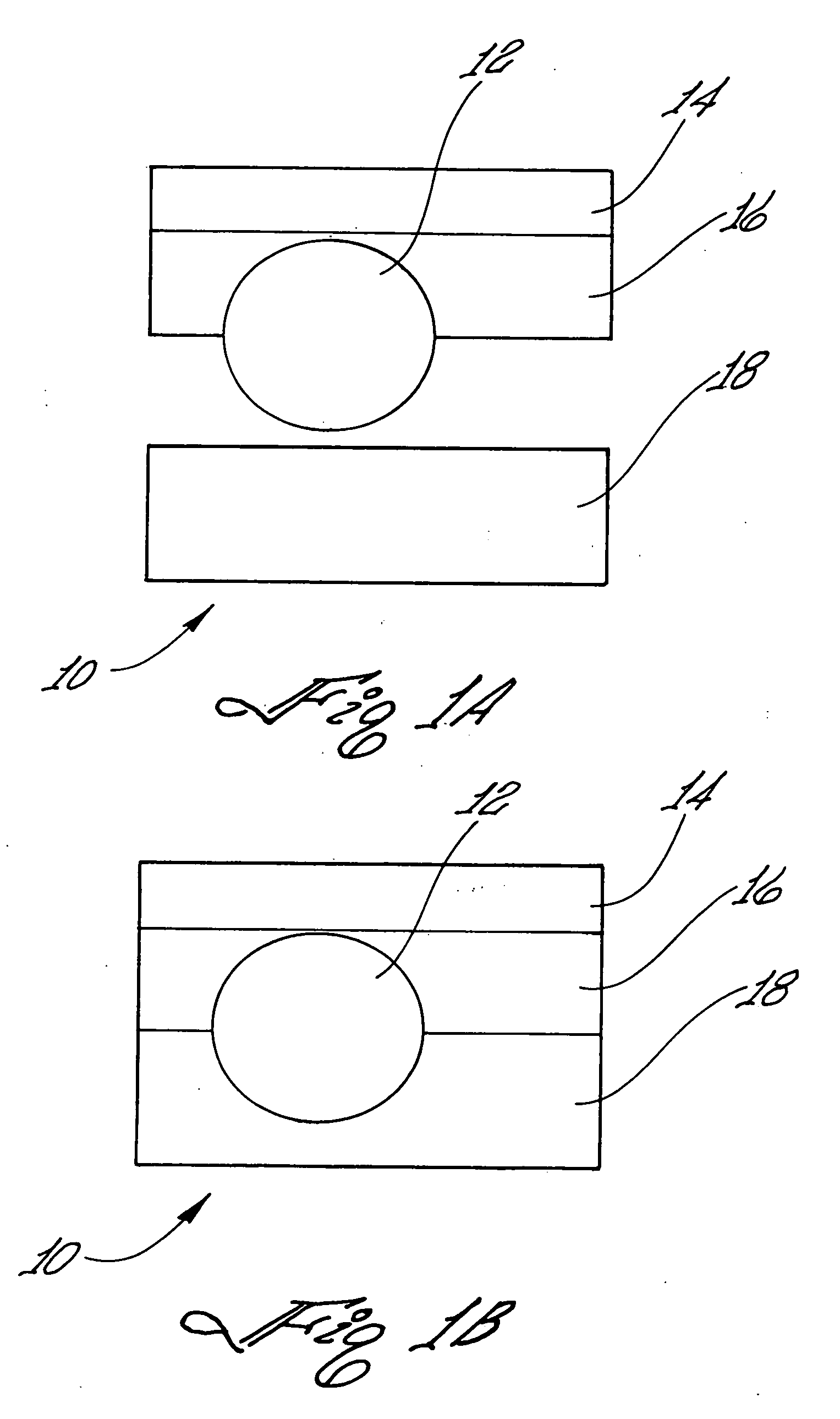
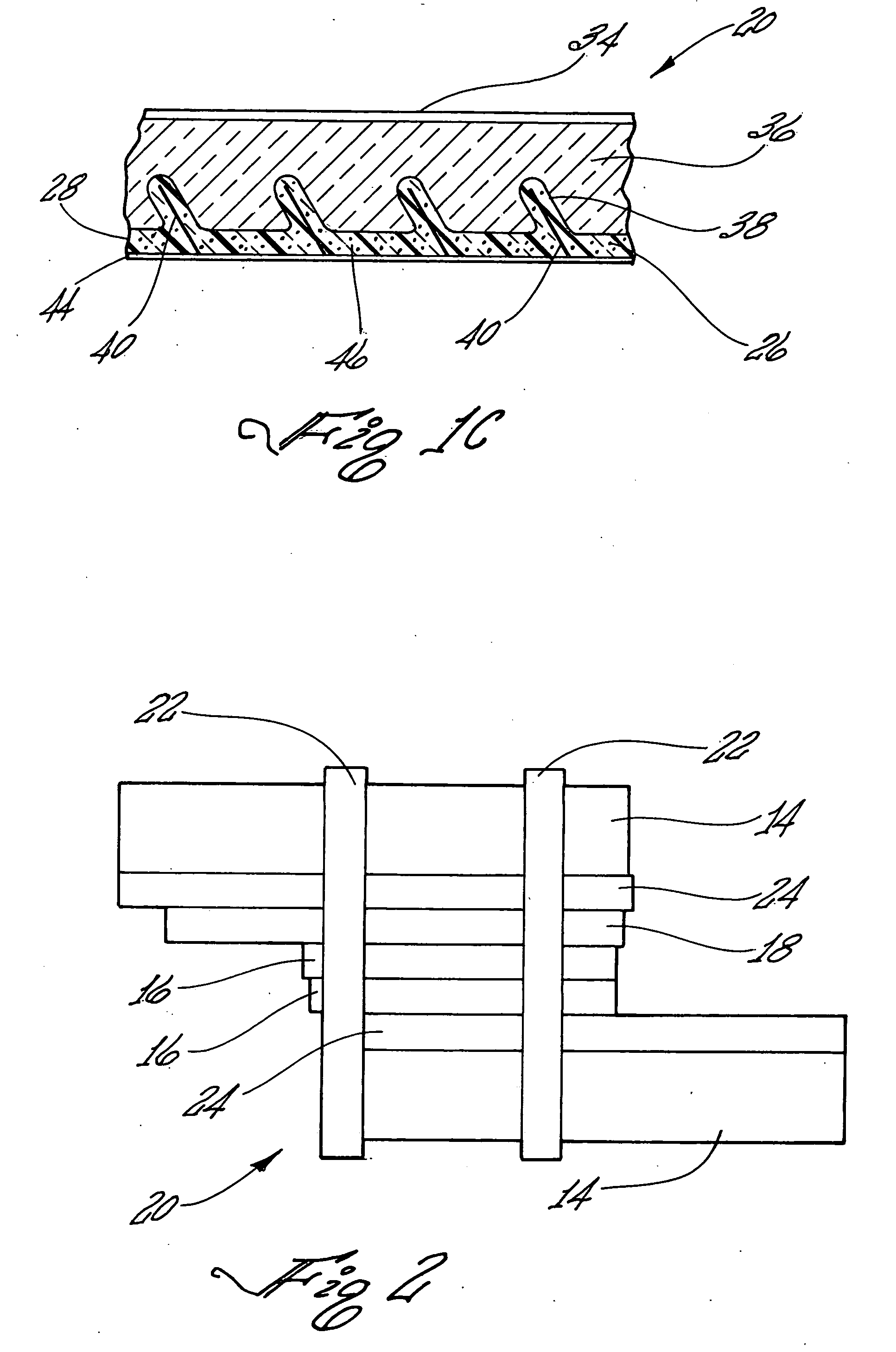
[0040] Substrates were prepared and cleaned. The preparation of the Sol-gel and conjugated polymer solutions were formulated and desired micro- and nano-structured molecules were dispersed in these solutions.

[0041] Substrates chosen for this embodiment were fluorine-doped tin oxide (SnO2:F) coated glass, purchased from Hartford Glass cut to size 3 inches by 1 inch. The substrates were cleaned by immersion in dilute alconox solution (detergent) at 50° C. for 1 hour, followed by rinsing with ultrapure water (17.9 Mega Ohm resistivity), isopropanol, chloroform, and absolute ethanol (absolute being 200 proof).

[0042] The sol-gel solution was prepared by mixing 9.8 mL ethanol (100%), 250 μL ultrapure H2O, and 1 drop of concentrated nitric acid (HN03) in a vial. It was desirable to include an alcohol and water mix ratio of about (1:0.025). Nitric acid was utilized for acidification of the alcohol / water mix. The vial was then transferred to a glove-box purged with N2 gas for approximately...


PUM

PropertyMeasurementUnit
widthaaaaaaaaaa
diameteraaaaaaaaaa
diameteraaaaaaaaaa

Abstract

A method of making films surface imprinted with nanometer-sized particles to produce micro- and/or nano-structured electron and hole collecting interfaces, include providing at least one transparent substrate, providing at least one photoabsorbing conjugated polymer, providing a sufficient amount of nanometer-sized particles to produce a charge separation interface, providing at least one transparent polymerizable layer, embedding the nanometer-sized particles in the conjugated polymer, applying the polymerizable layer and the conjugated polymer/nanometer-sized particle mixture on separate substrates where the nanometer-sized particles form a stamp surface, imprinting the stamp surface into the surface of the polymerizable film layer to produce micro- and/or nano-structured electron and hole collecting interfaces, polymerizing the polymerizable film layer to form a conformal gap, and filling the gap with at least one photoabsorbing material to promote the generation of photoexcited electrons and transport to the charge separation interface.

Description

[0001] This application is a continuation-in-part of U.S. patent application, Ser. No. 10 / 699,442, filed Oct. 29, 2003, and U.S. patent application Ser. No. 10 / 699,440, filed Oct. 29, 2003.STATEMENT REGARDING FEDERALLY SPONSORED RESEARCH OR DEVELOPMENT [0002] The invention described herein may be manufactured and used by or for the government of the United States of America for governmental purposes without the payment of any royalties thereon or therefor.BACKGROUND OF THE INVENTION [0003] 1. Field of the Invention. [0004] The present invention relates to apparatus and methods of surface imprinting films, and more specifically, films surface imprinted with nanometer-sized particles including multi-walled carbon nanotubes (MWNT) for military, commercial and recreational applications including, but not limited to, photovoltaic devices. [0005] 2. Description of the Prior Art. [0006] There is an ongoing worldwide effort within the field of nanotechnology to shrink the feature sizes of p...

Claims


Application Information

Patent Timeline
Patent Type & Authority Applications(United States)
IPC IPC(8): B29C39/12
CPCB82Y10/00Y10T156/1023H01L27/14665H01L51/0004H01L51/0036H01L51/0048H01L51/422H01L51/424H01L51/426H01L2251/105Y02E10/549Y10S977/773Y10S977/842Y10S977/778Y10T156/1041Y10T156/1044Y10T156/1039H01L27/14601H10K71/13H10K85/113H10K85/221H10K30/15H10K30/20H10K30/35H10K71/821B29C39/12
Inventor ROBERTS, M. JOSEPHJOHNSON, SCOTT K.HOLLINS, RICHARD A.JOHNSON, CURTIS E.GROSHENS, THOMAS J.IRVIN, DAVID J.
Owner THE UNITED STATES OF AMERICA AS REPRESENTED BY THE SECRETARY OF THE NAVY
Why Eureka
Try Eureka