Apparatus and method of via-stub resonance extinction

a technology of viastubs and resonances, applied in waveguide devices, multiple-port networks, final product manufacturing, etc., can solve the problems of limiting the electrical performance of both digital and analog systems, affecting signal integrity, and small features, so as to reduce the loss of reflection and flat frequency response

Inactive Publication Date: 2007-07-05
IBM CORP
View PDF3 Cites 24 Cited by
  • Summary
  • Abstract
  • Description
  • Claims
  • Application Information

AI Technical Summary

Benefits of technology

[0011] Reflection loss may also be reduced significantly at the resonance frequency. A resonance extinction resistor virtually converts a “non-working” link into a performance link without changing the PCB design and technology.
[0012] An apparatus includes a multi-layer printed circuit board having a first through-hole via for a signal connection and a second through hole via for power / ground connections. The printed circuit includes a transmission line connected to at least one through-hole via. A resistor is connected between the first and second through-hole vias to eliminate a resonance notch and achieve a flat frequency response for insertion loss when an integrated circuit chip is connected to the through-hole vias in operation.

Problems solved by technology

Electronic packaging has become a bottle neck that limits electrical performance of both digital and analog systems.
With the ever increasing operating speed / frequency or decrease in signal propagating wavelength, the effects of small features, which were negligible in the past, are now becoming critical and even detrimental to signal integrity.
One of the most significant examples is the vertical interconnects used in printed circuit boards (PCBs), also known as vias, which disturb electromagnetic wave propagation and therefore introduce transmission and reflection losses.
Further, when plated through holes (PTH) are used as in today's prevalent PCB technology and signal traces are connected intermittently, the excessive via-stub (section below signal layer) may introduce parasitic LC resonances and result in detrimental losses in the multi-GHz frequency range.
This jeopardizes signal integrity of such systems as servers, routers, etc.
However, back-drill not only increases cost but also affects mechanical stability of the board, and blind vias require a future technology and will result in much higher manufacturing costs.
The use of PTH vias tends to introduce excessive via sections or via stubs.
These LC resonances significantly increase insertion and reflection losses, and therefore become a main limiting factor for high-speed and multi-layer PCB applications.

Method used


Image

  • Apparatus and method of via-stub resonance extinction
  • Apparatus and method of via-stub resonance extinction
  • Apparatus and method of via-stub resonance extinction

Examples


Embodiment Construction

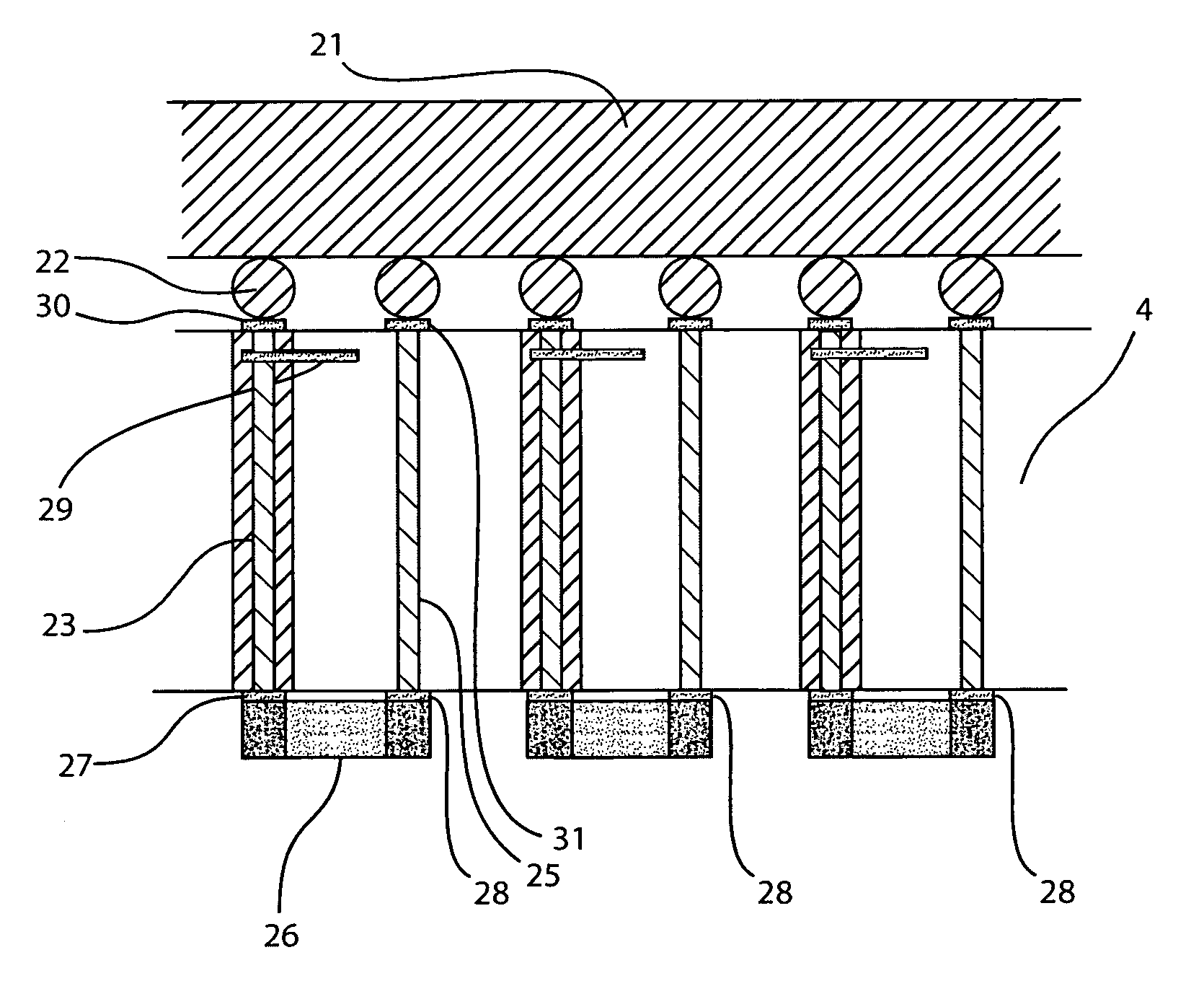
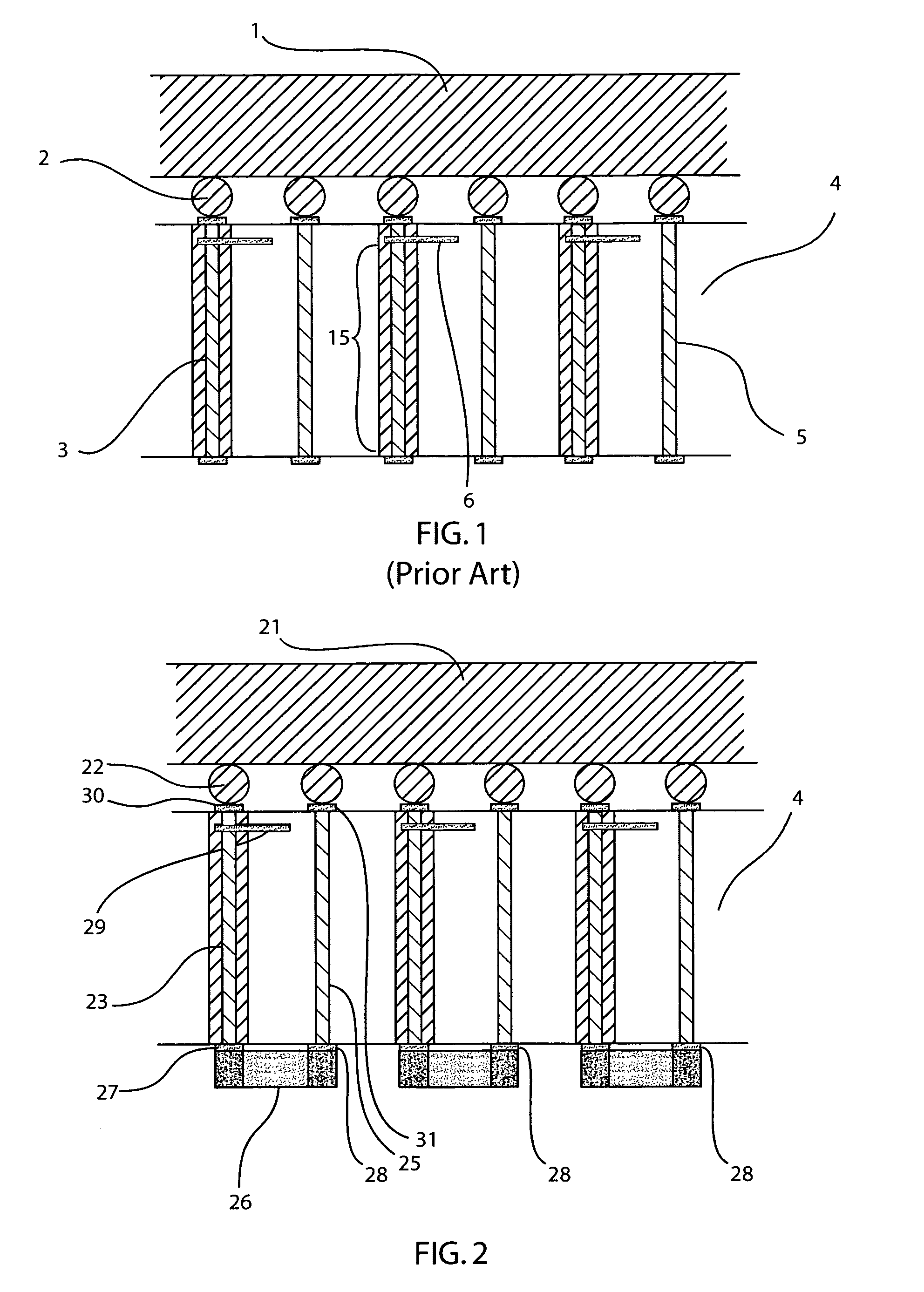
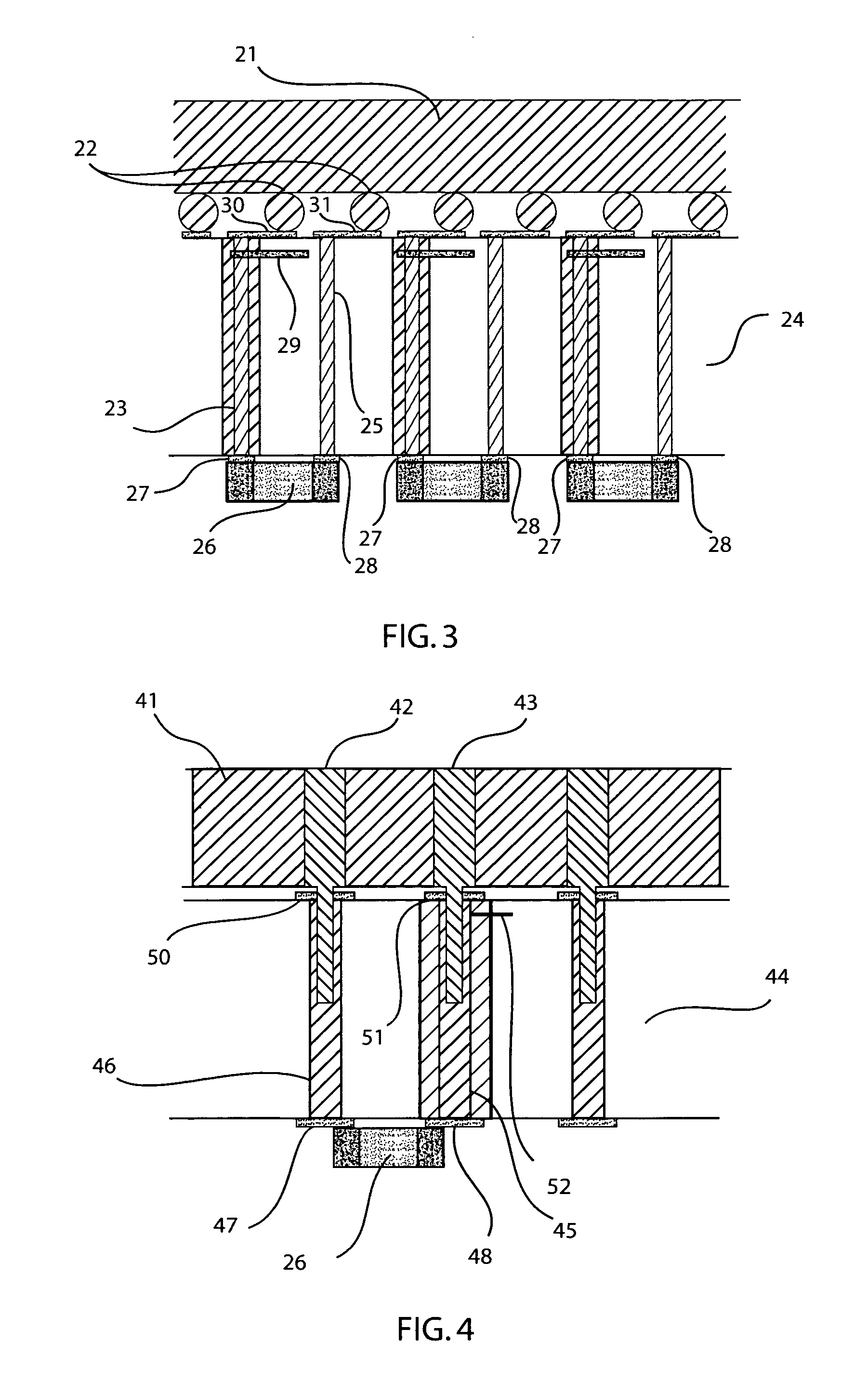
[0022] Exemplary embodiments of the present invention extinguish deep resonance notches due to via-stub LC resonance, so that both insertion loss and reflection may be reduced significantly, and electrical performance is improved. In one implementation, an extinction resistor is employed, which helps eliminate the resonance notch and achieve a desirable flat frequency response.

[0023] One application of such resonance extinction resistors employs surface-mount or integral resistors. In the case of surface-mount resistors, proper size and resistance may be used, and the resistor may be directly soldered onto existing external pads of a PCB, which guarantees backward compatibility.

[0024] As an example, in a via field of 1 mm pitch, which is common in existing packaging technologies, 0402 surface-mount resistors may be applied to a signal pad and an adjacent power / ground pad at the via-stub side (normally bottom side) without any modifications. Otherwise, additional solder pads may be...


PUM


Abstract

An apparatus includes a multi-layer printed circuit board having a first through-hole via for a signal connection and a second through hole via for power / ground connections. The printed circuit includes a transmission line connected to at least one through-hole via. A resistor is connected between the first and second through-hole vias to eliminate a resonance notch and achieve a flat frequency response for insertion loss.

Description

BACKGROUND [0001] 1. Technical Field [0002] The present invention relates to printed circuit boards (PCBS) and more particularly to improving electrical performance of PCBs with plated-through-holes (PTH) for connections among layers. [0003] 2. Description of the Related Art [0004] Electronic packaging has become a bottle neck that limits electrical performance of both digital and analog systems. With the ever increasing operating speed / frequency or decrease in signal propagating wavelength, the effects of small features, which were negligible in the past, are now becoming critical and even detrimental to signal integrity. One of the most significant examples is the vertical interconnects used in printed circuit boards (PCBs), also known as vias, which disturb electromagnetic wave propagation and therefore introduce transmission and reflection losses. [0005] Further, when plated through holes (PTH) are used as in today's prevalent PCB technology and signal traces are connected inter...

Claims


Application Information

Patent Timeline
Patent Type & Authority Applications(United States)
IPC IPC(8): H01P5/02
CPCH05K1/023H05K1/0246H05K1/112H05K3/429H05K2201/10734H05K2201/10022H05K2201/10545H05K2201/10636H05K2201/0792Y02P70/50
Inventor SHAN, LEITREWHELLA, JEANNINE
Owner IBM CORP
Why Eureka
Try Eureka