

Method for manufacturing single-walled carbon nanotube on glass
- Summary
- Abstract
- Description
- Claims
- Application Information
AI Technical Summary
Benefits of technology
Problems solved by technology
Method used
Image

Examples
example 1
[0036] A SiO2 thin film of about 200 nm in thickness was formed on a flat panel display glass (Corning 1737, manufactured by Samsung Corning Company Ltd.). In detail, while 30 W was applied to generate RF plasma, SiH4 with a gas flow of about 530 sccm and N2O with a gas flow of 320 sccm were introduced, respectively, and the SiO2 thin film was deposited on the flat panel display glass by a CVD method at almost 320° C.
[0037] Next, using a CoFe target (Co:Fe=9:1), the SiO2 thin film deposition process continued for 9 seconds with about 200 W RF plasma power by RF magnetron sputtering to form a 4.0 nm-thick CoFe catalytic layer on the buffer layer.
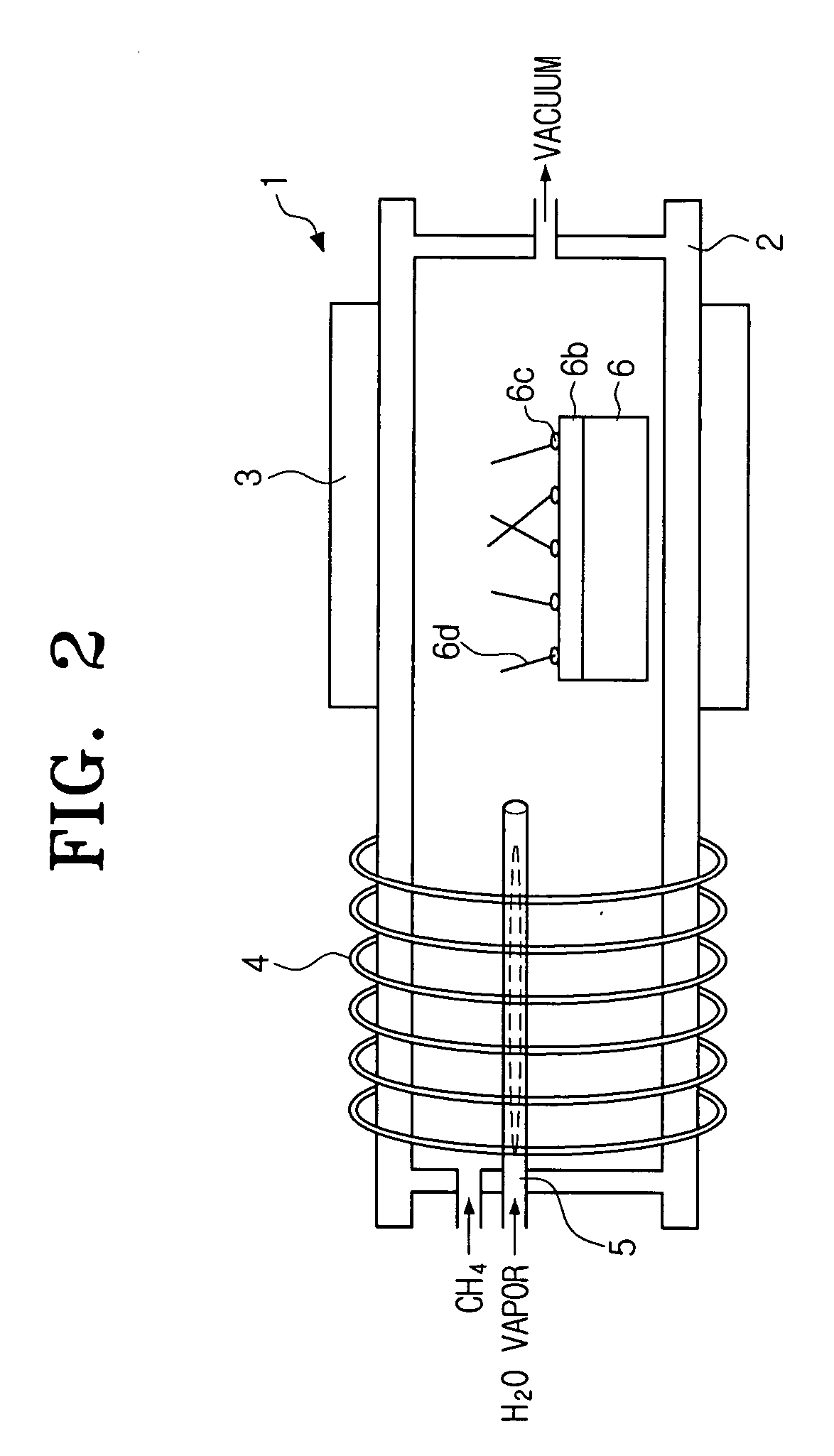
[0038] The glass substrate coated with the CoFe catalytic layer was then placed in the lamp-heating type radio frequency remote PECVD system shown in FIG. 2 for growing carbon nanotubes at a temperature of about 550° C. As for the source gas, methane gas with a gas flow of about 60 sccm was supplied to the system, and approximately 15 W was...
example 2
[0043] The same method as in Example 1 was used for growing carbon nanotubes, except that the SiO2 thin film deposition process was performed using a CoFe target (Co:Fe=9:1) for 10 seconds with about 50 W RF plasma power by RF magnetron sputtering, in order to form a 0.9 nm-thick CoFe catalytic layer on the buffer layer.
[0044]FIG. 6a is a transmission electron microscope (“TEM”) image of the CoFe catalytic layer, and FIG. 6e is an SEM image of the resulting carbon nanotube.
example 3
[0045] The same method as in Example 1 was used for growing carbon nanotubes, except that the SiO2 thin film deposition process was performed using a CoFe target (Co:Fe=9:1) for 10 seconds with about 70 W RF plasma power by RF magnetron sputtering, in order to form a 2.3 nm-thick CoFe catalytic layer on the buffer layer.
[0046]FIG. 6b is a TEM image of the CoFe catalytic layer, and FIG. 6f is an SEM image of the resulting carbon nanotube.
PUM
| Property | Measurement | Unit |
|---|---|---|
| Temperature | aaaaa | aaaaa |
| Temperature | aaaaa | aaaaa |
| Thickness | aaaaa | aaaaa |
Abstract
Description
Claims
Application Information